Global Wafer Cleaning Equipment Market By Equipment Type, By Technology, By Wafer Size, By Application, By End User, By Region, Competition, Forecast & Opportunities, 2021-2036F
Market Definition
The Global Wafer Cleaning Equipment Market covers the design, manufacture, supply, integration, and aftermarket service of precision semiconductor process tools used to remove organic residues, particulate contaminants, metallic impurities, native oxides, and post-etch and post-CMP polymer residues from silicon, silicon carbide, gallium nitride, and compound semiconductor wafers throughout the front-end-of-line and back-end-of-line fabrication workflow. The market includes single-wafer cleaning systems, batch immersion wet stations, batch spray cleaning tools, scrubber systems, cryogenic and supercritical CO2 cleaning equipment, and emerging dry plasma-based and laser-assisted cleaning platforms used across logic, memory, foundry, analog, power semiconductor, and advanced packaging production lines. Equipment is procured by integrated device manufacturers including Samsung, SK hynix, Micron, Intel, Texas Instruments, Infineon, STMicroelectronics, and Renesas, alongside pure-play foundries such as TSMC, GlobalFoundries, UMC, SMIC, Tower Semiconductor, and outsourced semiconductor assembly and test providers across the global semiconductor manufacturing ecosystem. The supplier landscape is concentrated among specialized wafer cleaning equipment vendors including SCREEN Semiconductor Solutions, Tokyo Electron, Lam Research, Applied Materials, ACM Research, SEMES, Veeco, and Naura Technology Group, with competition shaped by tool throughput, particle removal efficiency, defect performance at advanced nodes, chemical consumption, and integration compatibility with adjacent etch, deposition, and lithography process modules. Market dynamics are governed by capital expenditure cycles across leading-edge logic and memory fabs, technology transitions including EUV lithography adoption, 3D NAND layer scaling, gate-all-around transistor architectures, advanced packaging including 2.5D and 3D heterogeneous integration, and government incentive frameworks under the US CHIPS Act, the European Chips Act, and Asian semiconductor self-sufficiency programs.
Market Insights
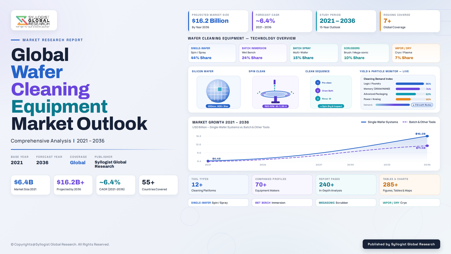
The global wafer cleaning equipment market is entering a sustained expansion cycle, propelled by accelerating leading-edge logic node transitions to 3 nm and 2 nm process geometries, vertical scaling of 3D NAND beyond 300 layers, the proliferation of advanced packaging architectures including 2.5D and 3D heterogeneous integration, and the structural capacity expansion under US CHIPS Act, European Chips Act, and Asia-Pacific semiconductor self-sufficiency programs. The market was valued at USD 11.4 billion in 2025 and is projected to reach USD 26.8 billion by 2034, advancing at a compound annual growth rate of 10.0% through the forecast period, as wafer cleaning steps proliferate within the integrated process flow and contamination control specifications tighten at every successive technology node.
Wafer cleaning has emerged as one of the most process-step-intensive segments of semiconductor fabrication, with leading-edge logic fabs executing over 200 distinct cleaning operations per wafer through the FEOL and BEOL flow, compared with approximately 80 cleaning steps at the 28 nm node a decade ago. Single-wafer cleaning platforms have displaced batch systems across critical front-end nodes given superior particle removal performance, defect uniformity, and chemical efficiency at sub-7 nm geometries, with single-wafer tools accounting for nearly 68% of incremental cleaning equipment shipments in 2025 and rising. Cryogenic aerosol cleaning, supercritical CO2 cleaning, and selective wet etch hybrid platforms are gaining commercial traction across EUV photoresist strip, high aspect ratio structure cleaning, and gate-all-around transistor channel preparation, with each technology transition introducing incremental tool demand across both new fab build-outs and node migration projects.
TSMC alone accounts for nearly 22% of global wafer cleaning equipment procurement in 2025, with capital expenditure exceeding USD 38 billion supporting Arizona, Kumamoto, Dresden, and Taiwan fab expansion programs that together require over 12,000 wafer cleaning tools across the construction pipeline. Samsung Foundry, SK hynix, Micron, Intel Foundry, and YMTC together represent the next layer of demand intensity, with combined wafer cleaning equipment procurement exceeding USD 4.2 billion in 2025 across Pyeongtaek, Hsinchu, Boise, Ohio, Magdeburg, and Wuhan facility expansions. Advanced packaging is emerging as a structurally important growth vector, with high-bandwidth memory production for AI accelerators, chiplet integration for data center GPUs, and 2.5D silicon interposer fabrication driving incremental cleaning tool demand at OSAT facilities operated by ASE Technology, Amkor, JCET, Powertech Technology, and SPIL across Taiwan, South Korea, China, Vietnam, and Malaysia.
Asia-Pacific dominates the global wafer cleaning equipment market with approximately 72% revenue share in 2025, anchored by Taiwan, South Korea, China, and Japan as the principal demand centers, with Japan also functioning as the dominant supplier base for advanced single-wafer cleaning platforms through SCREEN Semiconductor Solutions and Tokyo Electron. China is the fastest growing regional market, advancing at over 14% CAGR through 2034, as Yangtze Memory Technologies, ChangXin Memory Technologies, SMIC, Hua Hong Semiconductor, and Naura-supported domestic fab projects scale mature node and trailing-edge memory capacity under semiconductor self-sufficiency mandates. North America is rebuilding its share through CHIPS Act incentivized fab projects at Intel Ohio, TSMC Arizona, Samsung Taylor, Micron Boise and Syracuse, and GlobalFoundries Malta, while Europe is advancing capacity additions at TSMC Dresden, Intel Magdeburg, Infineon Villach, and STMicroelectronics Catania.
Key Drivers
Advanced Node Transitions to 3 nm, 2 nm, and Sub-2 nm Architectures Multiplying Wafer Cleaning Step Density and Equipment Demand
Each successive logic node transition is materially increasing wafer cleaning step density, with leading-edge fabs at 3 nm and 2 nm executing over 200 cleaning operations per wafer compared with approximately 120 at the 14 nm node, driven by tighter particle specifications, gate-all-around transistor process complexity, EUV photoresist residue removal, and increasingly complex multi-patterning workflows. TSMC, Samsung, and Intel Foundry capital programs targeting 2 nm and Angstrom-class production at Hsinchu, Pyeongtaek, and Ohio fabs are anchoring durable single-wafer cleaning tool demand, with each new leading-edge fab module requiring 200 to 300 cleaning systems.
3D NAND Layer Scaling, High-Bandwidth Memory Expansion, and DRAM Density Growth Driving Memory Fab Cleaning Tool Procurement
Vertical scaling of 3D NAND beyond 300 layers, high-bandwidth memory production ramping at SK hynix, Samsung, and Micron in support of AI accelerator demand, and DRAM density transitions to 1b nanometer and 1c nanometer nodes are driving sustained wafer cleaning equipment procurement across memory fabs. High aspect ratio structure cleaning, channel hole preparation, and through-silicon via cleaning for HBM stacks each require dedicated single-wafer and specialized cleaning platforms, with memory fab wafer cleaning equipment spend projected to advance at 11.6% CAGR through 2034.
Advanced Packaging, Heterogeneous Integration, and OSAT Capacity Expansion Generating Incremental Cleaning Tool Demand
Advanced packaging adoption including CoWoS, FOWLP, FOPLP, 2.5D silicon interposers, and 3D chiplet stacking is generating incremental wafer cleaning equipment demand, with TSMC, ASE Technology, Amkor, and JCET advancing CoWoS, SoIC, and panel-level packaging capacity targeting over USD 18 billion of cumulative capital deployment through 2030. Each advanced packaging line incorporates 30 to 60 cleaning steps including post-bonding particle removal, redistribution layer cleaning, and underfill preparation, anchoring durable equipment procurement across the OSAT ecosystem.
Key Challenges
US Export Controls on Advanced Semiconductor Equipment Shipments to China Constraining Supplier Revenue and Reshaping Trade Architecture
US Department of Commerce export controls covering advanced semiconductor manufacturing equipment shipments to China, expanded across 2022, 2023, and 2024 to include sub-14 nm logic and advanced memory production tools, are materially constraining wafer cleaning equipment supplier revenue exposure to Chinese leading-edge fabs and reshaping trade architecture. Applied Materials, Lam Research, KLA, and ASML have each disclosed China revenue reductions ranging from 18% to 32%, while ACM Research and Naura have expanded share in trailing-edge cleaning as Chinese fabs accelerate domestic supplier qualification.
Capital Expenditure Cyclicality, Inventory Adjustments, and Memory Market Volatility Introducing Equipment Procurement Lumpiness
Semiconductor capital expenditure remains structurally cyclical, with downcycles in 2023 reducing global wafer cleaning equipment shipments by nearly 11% year-over-year, driven by NAND and DRAM oversupply, inventory correction across consumer electronics, and capacity utilization declines below 75% across multiple memory operators. Memory market volatility, geopolitical demand uncertainty across mobile and consumer end markets, and capital allocation discipline at integrated device manufacturers are introducing procurement lumpiness that complicates production planning, supply chain management, and capacity utilization at equipment suppliers.
Skilled Workforce Shortages, Tool Installation Bottlenecks, and Aftermarket Service Capacity Constraints Limiting Fab Ramp Timelines
Structural shortages of semiconductor process engineers, field service engineers, and skilled fab technicians across North America, Europe, and emerging Asia-Pacific fab locations are extending wafer cleaning tool installation timelines, delaying fab qualification cycles, and constraining the ramp of new CHIPS Act and European Chips Act funded projects. Aftermarket service capacity, spare parts supply chain resilience, and tool calibration expertise availability remain critical bottlenecks, with TSMC Arizona, Intel Ohio, and Samsung Taylor all reporting fab ramp timeline extensions partially attributable to equipment installation and qualification capacity constraints.
Market Segmentation
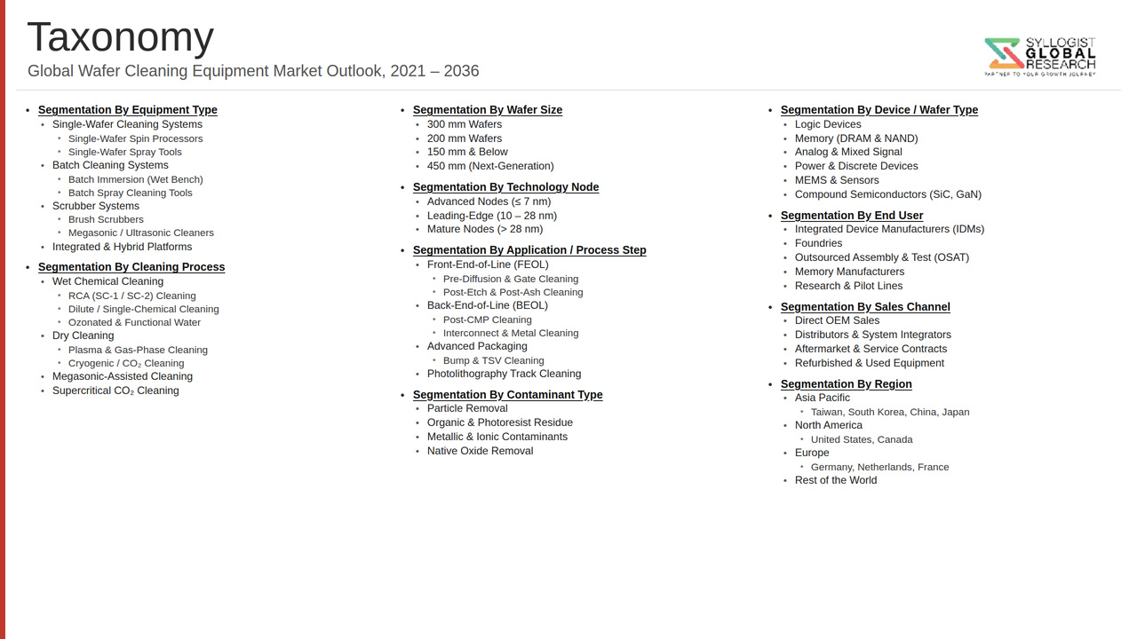
- Segmentation By Equipment Type
- Single-Wafer Cleaning Systems
- Batch Immersion Wet Stations
- Batch Spray Cleaning Tools
- Scrubber Systems
- Cryogenic Aerosol Cleaning Equipment
- Supercritical CO2 Cleaning Systems
- Dry Plasma and Laser-Assisted Cleaning Platforms
- Others
- Segmentation By Technology
- Wet Chemical Cleaning
- Dry Plasma Cleaning
- Megasonic and Ultrasonic Cleaning
- Cryogenic Aerosol Cleaning
- Supercritical CO2 Cleaning
- Laser and UV-Assisted Cleaning
- Others
- Segmentation By Wafer Size
- 150 mm and Below
- 200 mm
- 300 mm
- Emerging 450 mm and Panel Substrates
- Others
- Segmentation By Application
- Front-End-of-Line (FEOL) Cleaning
- Back-End-of-Line (BEOL) Cleaning
- Post-CMP Cleaning
- Post-Etch Residue Removal
- Photoresist Strip and Post-Strip Cleaning
- Advanced Packaging Cleaning
- Others
- Segmentation By End User
- Logic and Foundry
- Memory (DRAM, NAND, HBM)
- Analog and Mixed-Signal
- Power Semiconductors (SiC, GaN, Silicon)
- Compound Semiconductors and Optoelectronics
- MEMS and Sensors
- Outsourced Semiconductor Assembly and Test (OSAT)
- Others
- Segmentation By Region
- North America
- Europe
- Asia-Pacific (Taiwan, South Korea, China, Japan, Southeast Asia)
- Middle East and Africa
- Latin America
All market revenues are presented in USD
Historical Year: 2021-2024 | Base Year: 2025 | Estimated Year: 2026 | Forecast Period: 2027-2034
Key Questions this Study Will Answer
- What is the total market valuation of the Global Wafer Cleaning Equipment Market in 2025, projected through 2034, disaggregated by equipment type, technology, and end-user segment, enabling semiconductor equipment vendors, fab operators, OSAT providers, and investors to identify the highest-growth opportunities and most durable revenue corridors across the wafer cleaning value chain?
- How are advanced node transitions to 3 nm, 2 nm, and sub-2 nm geometries, gate-all-around transistor architectures, EUV adoption, and multi-patterning workflows multiplying wafer cleaning step density and reshaping single-wafer cleaning equipment demand across TSMC, Samsung Foundry, Intel Foundry, and leading-edge memory operators through 2034?
- Which wafer cleaning equipment categories including single-wafer cleaning systems, batch wet stations, scrubbers, cryogenic aerosol, supercritical CO2, and dry plasma platforms are generating the highest growth rates, and how are technology transitions reshaping competitive positioning across SCREEN, Tokyo Electron, Lam Research, Applied Materials, ACM Research, SEMES, and Naura?
- How are US export controls on advanced semiconductor manufacturing equipment shipments to China reshaping supplier revenue exposure, market share dynamics, and competitive positioning across leading-edge and trailing-edge wafer cleaning equipment categories, and how are Chinese domestic suppliers capturing share through 2034?
- How are CHIPS Act, European Chips Act, and Asia-Pacific semiconductor self-sufficiency programs driving wafer cleaning equipment procurement across Arizona, Ohio, Taylor, Boise, Magdeburg, Dresden, Kumamoto, Hsinchu, Pyeongtaek, and Chinese fab projects, and what regional demand patterns are emerging through 2034?
- How is advanced packaging adoption including CoWoS, SoIC, FOWLP, FOPLP, 2.5D silicon interposers, and 3D heterogeneous integration generating incremental wafer cleaning equipment demand at OSAT facilities operated by ASE Technology, Amkor, JCET, Powertech Technology, and SPIL, and what cleaning step density is each packaging architecture introducing?
- How is the competitive landscape structured among leading wafer cleaning equipment suppliers including SCREEN Semiconductor Solutions, Tokyo Electron, Lam Research, Applied Materials, ACM Research, SEMES, Veeco, and Naura Technology Group, and what partnership, technology licensing, and capacity expansion strategies are reshaping market share dynamics through 2034?
- Product Definition
- Research Methodology
- Research Design & Framework
- Overall Research Approach: Descriptive, Exploratory & Quantitative Mixed-Method Design
- Market Definition & Scope Boundaries: What is Included and Excluded
- Segmentation Framework
- Key Research Assumptions & Limitations
- Secondary Research
- Primary Research Design & Execution
- Data Triangulation & Validation
- Market Sizing & Forecasting Methodology
- Competitive Intelligence Methodology
- Quality Assurance & Peer Review
- Definitions, Abbreviations & Data Notes
- Research Design & Framework
- Executive Summary
- Market Snapshot & Headline Numbers
- Key Findings & Research Highlights
- Market Dynamics
- Regional Market Summary
- Competitive Landscape Snapshot
- Technology & Innovation Highlights
- Market Dynamics
- Drivers
- Restraints
- Opportunities
- Challenges
- Porter’s Five Forces Analysis
- PESTLE Analysis
- Market Trends & Developments
- Emerging Trends
- Technological Developments
- Regulatory & Policy Changes
- Supply Chain & Sourcing Trends
- Manufacturing & Process Trends
- Investment & Funding Activity
- Sustainability & ESG Trends
- Risk Assessment Framework
- Semiconductor Capex Cyclicality, Fab Investment Slowdown & Order Book Volatility Risk
- Geopolitical Tension, Export Control, Chip War & Cross-Border Technology Transfer Risk
- Process Chemical, Ultrapure Water & Specialty Gas Supply Chain Risk
- Technology Node Transition, 3D Architecture & High-NA EUV Cleaning Integration Risk
- Capital Intensity, Equipment Qualification & Stranded Tool Risk
- Regulatory Framework & Standards
- SEMI Standards (E168, F47, S2, S8) & International Equipment Safety, Reliability & Productivity Frameworks
- Export Control Regulations: US Entity List, BIS, EAR, Wassenaar Arrangement & Semiconductor Equipment Trade Restrictions
- Hazardous Chemical, HF Handling, Sulfuric Acid & Specialty Solvent Safety Standards
- Cleanroom (ISO 14644), Ultrapure Water (ASTM, SEMI F63) & Wastewater Treatment Standards
- Energy Efficiency, Chemical Reduction, Green Fab & ESG Disclosure Standards for Semiconductor Equipment
- Global Wafer Cleaning Equipment Market Outlook
- Market Size & Forecast by Value
- Market Size & Forecast by Volume (Units / Tool Installations)
- Market Size & Forecast by Equipment Type
- Single-Wafer Cleaning Systems
- Batch Immersion & Spray Cleaning Systems
- Spin-Spray Cleaning Systems
- Megasonic & Ultrasonic Cleaning Systems
- Cryogenic CO2 & Aerosol Cleaning Systems
- Dry & Plasma-Based Cleaning Systems
- Post-CMP Brush Scrubber Systems
- Bevel, Edge & Backside Cleaning Systems
- Supercritical CO2 Cleaning Systems
- Market Size & Forecast by Cleaning Technology
- Wet Chemical Cleaning (SPM, APM, HPM & RCA SC1/SC2)
- Single-Wafer Spin Cleaning Technology
- Batch Immersion & Tank Cleaning Technology
- Megasonic-Assisted Wet Cleaning Technology
- Dry Plasma & Reactive Gas Cleaning Technology
- UV-Ozone & Photochemical Cleaning Technology
- Cryogenic Aerosol & Supercritical CO2 Cleaning Technology
- Vapor Phase HF & Chemical Vapor Cleaning Technology
- Post-CMP Brush, Pad & Slurry Removal Cleaning Technology
- Market Size & Forecast by Wafer Size
- Sub-200mm Wafer Cleaning Equipment
- 200mm (8-inch) Wafer Cleaning Equipment
- 300mm (12-inch) Wafer Cleaning Equipment
- Compound Semiconductor Wafer Cleaning Equipment (SiC, GaN, GaAs)
- 450mm & Next-Generation Wafer Cleaning Equipment
- Market Size & Forecast by Process Step / Application
- Front-End-of-Line (FEOL) Cleaning (Gate Stack, STI & Pre-Diffusion)
- Back-End-of-Line (BEOL) Cleaning (Interconnect & Damascene)
- Post-Etch Residue Removal
- Post-CMP Cleaning
- Photoresist Strip, Ashing & Post-Ash Cleaning
- Post-Implantation Cleaning
- Bevel, Edge & Backside Particle Removal
- Final Clean & Wafer Bonding Preparation
- Market Size & Forecast by Technology Node
- Mature Nodes (Above 28nm)
- Advanced Mature Nodes (28nm to 14nm)
- Advanced Nodes (10nm to 5nm)
- Leading-Edge Nodes (3nm, 2nm & Below)
- 3D NAND & Advanced Memory Nodes
- Market Size & Forecast by Device Type
- Logic ICs (CPU, GPU, SoC & Application Processors)
- Memory Devices (DRAM, 3D NAND & Emerging Memory)
- Analog, Mixed-Signal & RF Devices
- Power Semiconductors (Silicon, SiC & GaN)
- MEMS & Sensors
- Photonics & Silicon Photonics
- Discrete Devices & Optoelectronics (LED, Laser Diodes)
- Compound Semiconductor & Advanced Packaging Substrates
- Market Size & Forecast by End-User
- Integrated Device Manufacturers (IDMs)
- Pure-Play Foundries
- Memory Manufacturers
- Outsourced Semiconductor Assembly & Test (OSAT) Providers
- Compound Semiconductor & Power Device Fabs
- MEMS, Photonics & Specialty Foundries
- Research Institutes, Universities & Pilot Lines
- Market Size & Forecast by Sales Channel
- New Equipment Sales (OEM Direct)
- Refurbished & Pre-Owned Equipment Sales
- Aftermarket, Spares, Consumables & Service Contract
- Distributor & Regional Sales Partner Channel
- North America Wafer Cleaning Equipment Market Outlook
- Market Size & Forecast
- By Value
- By Volume (Units / Tool Installations)
- By Equipment Type
- By Cleaning Technology
- By Wafer Size
- By Process Step / Application
- By Technology Node
- By Device Type
- By End-User
- By Country
- By Sales Channel
- Europe Wafer Cleaning Equipment Market Outlook
- Market Size & Forecast
- By Value
- By Volume (Units / Tool Installations)
- By Equipment Type
- By Cleaning Technology
- By Wafer Size
- By Process Step / Application
- By Technology Node
- By Device Type
- By End-User
- By Country
- By Sales Channel
- Asia-Pacific Wafer Cleaning Equipment Market Outlook
- Market Size & Forecast
- By Value
- By Volume (Units / Tool Installations)
- By Equipment Type
- By Cleaning Technology
- By Wafer Size
- By Process Step / Application
- By Technology Node
- By Device Type
- By End-User
- By Country
- By Sales Channel
- Latin America Wafer Cleaning Equipment Market Outlook
- Market Size & Forecast
- By Value
- By Volume (Units / Tool Installations)
- By Equipment Type
- By Cleaning Technology
- By Wafer Size
- By Process Step / Application
- By Technology Node
- By Device Type
- By End-User
- By Country
- By Sales Channel
- Middle East & Africa Wafer Cleaning Equipment Market Outlook
- Market Size & Forecast
- By Value
- By Volume (Units / Tool Installations)
- By Equipment Type
- By Cleaning Technology
- By Wafer Size
- By Process Step / Application
- By Technology Node
- By Device Type
- By End-User
- By Country
- By Sales Channel
- Country-Wise* Wafer Cleaning Equipment Market Outlook
- Market Size & Forecast
- By Value
- By Volume (Units / Tool Installations)
- By Equipment Type
- By Cleaning Technology
- By Wafer Size
- By Process Step / Application
- By Technology Node
- By Device Type
- By End-User
- By Country
- By Sales Channel
- *Countries Analyzed in the Syllogist Global Research Portfolio: United States, Canada, Mexico, Germany, France, United Kingdom, Netherlands, Spain, Italy, Norway, Sweden, China, Japan, India, Australia, South Korea, Singapore, Taiwan, Brazil, Chile, Saudi Arabia, UAE, Egypt, South Africa, Israel
- Technology Landscape & Innovation Analysis
- Single-Wafer Cleaning Technology Deep-Dive: Chamber Design, Chemistry Delivery & Particle Performance
- Megasonic, Acoustic & Cavitation-Based Cleaning Technology for Sub-5nm Pattern Damage Control
- Dry, Plasma, UV-Ozone & Reactive Gas Cleaning Technology
- Cryogenic Aerosol, Supercritical CO2 & Solvent-Free Cleaning Technology
- Post-CMP Brush, Pad & Slurry Removal Cleaning Technology
- Bevel, Edge, Backside & Particle Defect Reduction Cleaning Technology
- Compound Semiconductor (SiC, GaN, GaAs) Wafer Cleaning Technology
- AI-Driven Process Control, Sensor Integration & Predictive Maintenance Technology
- Patent & IP Landscape in Wafer Cleaning Equipment Technologies
- Value Chain & Supply Chain Analysis
- Wafer Cleaning Equipment OEM Manufacturing & Component Supply Chain
- Specialty Chemical, Ultrapure Water & Process Gas Supply Chain
- Robotics, Wafer Handling, Vacuum & Motion Control Subsystem Supply Chain
- Pump, Filtration, Valve & Fluid Handling Component Supply Chain
- IDM, Foundry & OSAT Procurement & Equipment Qualification Landscape
- Refurbished Equipment, Aftermarket Service & Spare Parts Channel
- End-of-Life Tool Decommissioning, Recycling & Circular Economy
- Pricing Analysis
- Single-Wafer Cleaning System Capital Cost & Cost-of-Ownership Analysis
- Batch Wet Cleaning System Capital and Operating Cost Analysis
- Dry, Plasma & Cryogenic Cleaning System Pricing Analysis
- Post-CMP Cleaning System Cost & Throughput Economics Analysis
- Aftermarket, Spares, Consumables & Service Contract Revenue Analysis
- Total Cost-of-Ownership: Equipment, Chemicals, Water, Energy & Yield Co-Optimisation Analysis
- Sustainability & Environmental Analysis
- Lifecycle Assessment (LCA) of Wafer Cleaning Equipment: Carbon Footprint, Chemical Intensity & Water Footprint Across Tool Types
- Process Chemical Reduction, Solvent Substitution & Green Chemistry Pathway for Wafer Cleaning
- Ultrapure Water Conservation, Recycling & Wastewater Treatment in Fab Operations
- Energy Efficiency, Heat Recovery & Net Zero Fab Contribution of Cleaning Equipment
- Regulatory-Driven Sustainability, PFAS Phase-Out, Green Fab Standards & ESG Disclosure Alignment
- Competitive Landscape
- Market Structure & Concentration
- Market Consolidation Level (Fragmented vs. Consolidated by Equipment Type & Geography)
- Top 10 Players Market Share
- HHI (Herfindahl-Hirschman Index) Concentration Analysis
- Competitive Intensity Map by Equipment Type, Technology Node & Geography
- Player Classification
- Integrated Semiconductor Equipment Majors (Tokyo Electron, Lam Research, Applied Materials)
- Specialist Wafer Cleaning Equipment OEMs (SCREEN Holdings, ACM Research, SEMES, Kingsemi)
- Post-CMP & Brush Scrubber Specialists
- Dry, Plasma & Cryogenic Cleaning Technology Providers
- Compound Semiconductor (SiC, GaN) Cleaning Equipment Specialists
- Refurbished, Pre-Owned & Aftermarket Service Companies
- Robotics, Wafer Handling & Subsystem Integrators
- Process Chemical, Ultrapure Water & Consumables Supplier Partners
- Competitive Analysis Frameworks
- Market Share Analysis by Equipment Type, Technology Node & Region
- Company Profile
- Company Overview & Headquarters
- Wafer Cleaning Equipment Products & Technology Portfolio
- Key Customer Relationships & Reference Fab Installations
- Manufacturing Footprint & Production Capacity
- Revenue (Wafer Cleaning Equipment Segment) & Backlog
- Technology Differentiators & IP
- Key Strategic Partnerships, JVs & M&A Activity
- Recent Developments (Tool Wins, Capacity Expansion, Product Launches)
- SWOT Analysis
- Strategic Focus Areas & Roadmap
- Competitive Positioning Map (Technology Capability vs. Market Penetration)
- Key Company Profiles
- Market Structure & Concentration
- Technology Landscape & Innovation Analysis
- Strategic Output
- Market Opportunity Matrix: By Equipment Type, Cleaning Technology, Process Step, End-User & Geography
- White Space Opportunity Analysis
- Strategic Recommendations
- Product Portfolio & Technology Investment Strategy
- Manufacturing & Operational Excellence Strategy
- Geographic Expansion & Localisation Strategy
- Customer, Fab & End-User Engagement Strategy
- Partnership, M&A & Ecosystem Strategy
- Sustainability & Circular Economy Strategy
- Risk Mitigation & Future Roadmap
- Strategic Priority Matrix & Roadmap
- Near-term (2025-2028)
- Mid-term (2029-2032)
- Long-term (2033-2037)
- Market Size & Forecast
- Market Size & Forecast
- Market Size & Forecast
- Market Size & Forecast
- Market Size & Forecast
- Market Size & Forecast