Market Definition
The Global 3D IC and Chiplet Architecture Market encompasses the design, engineering, fabrication, packaging, testing, and commercial deployment of advanced semiconductor integration technologies that stack, interconnect, and combine multiple discrete die or functional chiplets within a single package to achieve system-level performance, bandwidth, power efficiency, and form factor outcomes that cannot be realized through conventional monolithic system-on-chip integration on a single continuous silicon substrate. Three-dimensional integrated circuit technology involves the vertical stacking of two or more semiconductor die using through-silicon vias, hybrid bonding, micro-bump interconnects, or direct copper-to-copper bonding at face-to-face or face-to-back orientations to create stacked memory-on-logic, logic-on-logic, and heterogeneous sensor-logic integration structures that dramatically increase inter-die communication bandwidth, reduce interconnect latency and power consumption relative to package-level die-to-die connections, and enable the integration of dissimilar semiconductor technologies including memory, logic, analog, and photonic components fabricated on process nodes optimized for each functional layer. Chiplet architecture extends the integration philosophy to a modular disaggregated system design paradigm in which a complex system-on-chip is decomposed into a collection of smaller, individually optimized, and separately fabricated functional die, termed chiplets, that are integrated within an advanced package using high-density interconnect substrates including silicon interposers, organic redistributed layer substrates, silicon bridges, embedded multi-die interconnect bridges, and active interposers, with each chiplet fabricated on the optimal process node for its function rather than constraining all functions to a single process technology. The market encompasses through-silicon via formation, hybrid bonding processes including direct bonded interconnect technology, advanced packaging substrates, chip-on-wafer-on-substrate, wafer-on-wafer, fan-out wafer-level packaging, and system-in-package architectures, as well as the design automation, thermal management, testing, and known-good-die infrastructure essential to commercial chiplet ecosystem viability. Key participants include integrated device manufacturers, foundries, outsourced semiconductor assembly and test providers, substrate manufacturers, electronic design automation tool developers, and hyperscaler, artificial intelligence, and high-performance computing customers driving adoption.
Market Insights
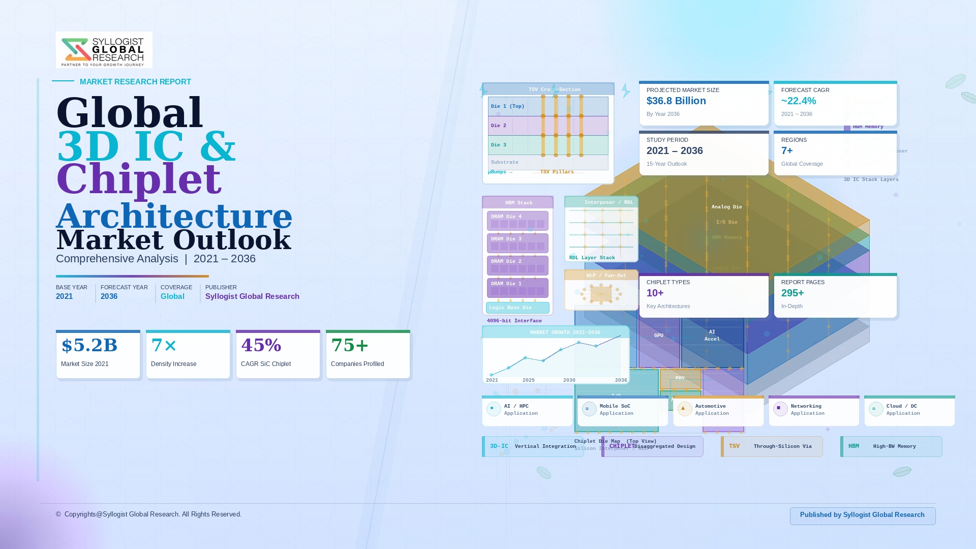
The global 3D IC and chiplet architecture market was valued at approximately USD 18.4 billion in 2025 and is projected to reach USD 78.6 billion by 2034, advancing at a compound annual growth rate of 17.4% over the forecast period from 2027 to 2034, driven by the physical and economic limitations of conventional monolithic scaling on a single process node that are compelling the semiconductor industry to pursue heterogeneous integration as the primary pathway for continued system performance improvement beyond the capabilities of leading-edge two-dimensional transistor scaling alone. The end of Dennard scaling, which historically allowed transistor count doubling to deliver proportional power density improvement, has created a fundamental inflection point where continued monolithic integration of more transistors on larger die at advanced nodes generates diminishing returns in system power efficiency, yields degrading proportionally with die area at the most advanced process nodes, and reticle-limited die size constraints that prevent the integration of sufficient compute, memory bandwidth, and input-output capacity within a single monolithic die to satisfy the insatiable bandwidth and compute density requirements of artificial intelligence training and inference accelerators, high-performance computing processors, and next-generation networking chips whose system requirements have definitively outgrown what any single reticle-limited die can contain. The artificial intelligence hardware market is the primary commercial catalyst for 3D IC and chiplet adoption at scale, with NVIDIA’s H100 and H200 graphics processing units utilizing high-bandwidth memory stacked directly on the package through silicon interposer integration consuming approximately 900 gigabytes per second of memory bandwidth per graphics processing unit that would be physically impossible to achieve with conventional dual in-line memory module connectivity, and AMD’s EPYC Genoa server processors utilizing chiplet architecture to integrate twelve compute die manufactured on TSMC’s 5-nanometer process with a central I/O die on a 6-nanometer node within a single package, demonstrating at commercial scale the system performance and manufacturing yield economics that chiplet disaggregation enables.
High-bandwidth memory stacked on silicon interposers represents the most commercially deployed and revenue-generating 3D IC integration technology within the global market, with high-bandwidth memory second generation, third generation, and fourth generation stacks combining four, eight, or twelve dynamic random-access memory die vertically through thousands of through-silicon vias per stack to deliver memory bandwidth of 307 gigabytes per second per stack for high-bandwidth memory second generation and approximately 1,200 gigabytes per second per stack for high-bandwidth memory fourth generation at dramatically lower power per bit than equivalent discrete memory solutions, enabling the artificial intelligence accelerator and graphics processing unit performance levels required for large language model training whose matrix multiplication operations are fundamentally memory-bandwidth-limited at the scale of hundreds of billions of parameters. SK Hynix delivered the first commercial high-bandwidth memory fourth generation production volumes to NVIDIA for integration into the H100 graphics processing unit in 2023, establishing high-bandwidth memory fourth generation as the enabling memory technology for the current generation of large language model training infrastructure, with Samsung and Micron following into high-bandwidth memory fourth generation production, and all three memory manufacturers competing in high-bandwidth memory fifth generation development targeting 1,500 gigabytes per second per stack bandwidth for next-generation artificial intelligence accelerator platforms expected to enter production between 2025 and 2027. The silicon interposer market supporting high-bandwidth memory and chiplet integration is dominated by TSMC’s chip-on-wafer-on-substrate process technology, with TSMC’s advanced packaging revenue reaching approximately USD 8.2 billion in 2025 and growing at approximately 32% annually as hyperscalers including Google, Amazon, Microsoft, and Meta adopt custom artificial intelligence accelerators utilizing chip-on-wafer-on-substrate and system-on-integrated-chip packaging technologies that require TSMC’s most advanced 3D integration process capabilities.
The chiplet ecosystem is evolving from a captive architecture used exclusively within individual company design portfolios toward an emerging open interconnect standard environment that could enable multi-vendor chiplet integration, with the Universal Chiplet Interconnect Express standard, developed by Intel and subsequently adopted by AMD, ARM, Qualcomm, Samsung, TSMC, and a growing coalition of semiconductor companies, providing a standardized die-to-die interconnect protocol specifying electrical, logical, and protocol layer requirements for chiplet-to-chiplet communication that is necessary to realize the full economic and design flexibility benefits of a modular chiplet ecosystem in which compute, memory, analog, and input-output chiplets from different vendors can be integrated within a customer-designed package without proprietary vendor lock-in. Intel’s Meteor Lake client processor released in late 2023 was the first mainstream client computing product to utilize a multi-chiplet architecture with die from different process nodes and different fabrication sources integrated on a foveros three-dimensional packaging platform, combining a compute tile manufactured on TSMC’s 4-nanometer process with an input-output tile on Intel’s 6-nanometer process and an SoC tile on TSMC’s 6-nanometer process within a single package, demonstrating commercial chiplet heterogeneous sourcing across multiple foundries that validates the technical feasibility of multi-source chiplet integration at high-volume consumer computing product scale. The thermal management challenge of three-dimensional die stacking, where heat generated by compute die stacked beneath memory or additional logic die cannot be efficiently conducted to package-level cooling solutions through the overlying die stack, is driving investment in advanced thermal interface materials, micro-channel liquid cooling integrated within die stacks, and thermal-aware three-dimensional floorplanning design methodologies that represent a growing engineering specialization within the 3D IC ecosystem whose commercial solutions are increasingly valued by customers pushing power density boundaries in artificial intelligence accelerator and high-performance computing chip design.
The competitive and supply chain landscape of the 3D IC and chiplet architecture market is defined by the critical positioning of a small number of advanced packaging technology leaders whose process capabilities represent strategic bottlenecks in the artificial intelligence hardware supply chain, with TSMC’s chip-on-wafer-on-substrate and system-on-integrated-chip advanced packaging technologies, Samsung Foundry’s X-Cube three-dimensional stacking process, and Intel Foundry Services’ foveros and embedded multi-die interconnect bridge packaging platforms each representing differentiated three-dimensional integration process portfolios that are increasingly factored into fabless semiconductor customer foundry selection decisions alongside front-end-of-line transistor performance and cost metrics. The outsourced semiconductor assembly and test sector is undergoing a strategic positioning transformation as the most technically sophisticated advanced packaging work gravitates toward front-end foundries with wafer-level processing capability for hybrid bonding and silicon interposer fabrication, while traditional assembly and test companies including ASE Group, Amkor Technology, JCET, and Powertech Technology are investing in fan-out wafer-level packaging, system-in-package, and chip-on-wafer assembly capabilities to capture the growing advanced packaging market segments that do not require silicon interposer or hybrid bonding processes. The known-good-die testing challenge, which requires each individual chiplet to be tested and verified at parametric performance before integration into a multi-chiplet package from which defective die cannot be replaced without complete package disassembly and reconstruction, is creating demand for advanced pre-bond testing methodologies, wafer-level burn-in screening, and die-level performance binning infrastructure whose cost and throughput characteristics materially influence the total system cost economics of chiplet-based designs relative to monolithic alternatives at different yield and complexity points.
Key Drivers
Insatiable Artificial Intelligence and High-Performance Computing Bandwidth and Compute Density Requirements Exceeding What Monolithic Die Integration Can Deliver Within Physical and Economic Constraints
The exponentially growing computational requirements of large language model training and inference, scientific simulation, genomics, and financial modeling workloads are creating system performance requirements that fundamentally exceed what monolithic single-die integration can deliver within reticle size constraints, acceptable die yield economics, and thermal dissipation boundaries at leading-edge process nodes, establishing 3D IC and chiplet architecture as the only technically viable pathway for continued system-level performance scaling for the most demanding artificial intelligence and high-performance computing applications through the forecast period. Training large language model systems at the scale of hundreds of billions of parameters requires compute clusters consuming petabytes per second of aggregate memory bandwidth, a requirement that translates at the chip level into graphics processing unit and artificial intelligence accelerator designs requiring eight or more high-bandwidth memory stacks per package delivering aggregate bandwidth exceeding 3,000 gigabytes per second per chip, bandwidth levels that are physically achievable only through through-silicon via-based high-bandwidth memory stacking on silicon interposers whose interconnect density creates orders-of-magnitude more memory-to-processor bandwidth per unit of package area than any conventional multi-chip package or dual in-line memory module connectivity solution. The economic driver reinforcing the technical case for chiplet disaggregation is the dramatic improvement in manufacturing yield economics achievable by decomposing a large monolithic die into smaller constituent chiplets, as yield on advanced process nodes scales inversely with die area following Poisson defect distribution statistics, meaning a 500-square-millimeter monolithic die at a node with 0.1 defects per square centimeter yields at approximately 61% while decomposing the equivalent functionality into four 125-square-millimeter chiplets yields each individual chiplet at approximately 88%, delivering a compound system yield of approximately 60% but enabling the replacement of individual known-bad chiplets rather than scrapping the entire package, fundamentally improving the economics of leading-edge semiconductor integration at system complexity levels demanded by current and next-generation artificial intelligence processor architectures.
Escalating Cost and Complexity of Advanced Node Monolithic Integration Compelling Process Node Disaggregation and Heterogeneous Multi-Technology Chiplet System Design
The escalating capital cost of leading-edge semiconductor fabrication at 3-nanometer, 2-nanometer, and beyond process nodes, combined with the diminishing performance and power improvement returns per node generation relative to earlier scaling eras, is compelling semiconductor design teams to adopt chiplet disaggregation strategies that allocate each functional subsystem of a complex chip to the most cost-effective and performance-optimal process node for that function rather than implementing all functions on the most advanced and most expensive available process technology. A state-of-the-art 2-nanometer logic transistor carries a wafer processing cost of approximately USD 20,000 to USD 25,000 per wafer, compared to approximately USD 3,000 to USD 4,000 per wafer for mature 28-nanometer node processing, creating a compelling economic rationale for implementing input-output interfaces, analog circuits, power management, and other functions whose performance does not benefit from leading-edge transistor scaling on mature process nodes at a fraction of the per-transistor cost of advanced nodes, while concentrating expensive advanced node silicon area exclusively in the compute-intensive logic functions where transistor performance directly translates into system capability improvement. AMD’s EPYC server processor chiplet strategy, which disaggregates compute cores onto small high-yield 5-nanometer chiplets while implementing the input-output die on a larger but less costly 6-nanometer process node, has demonstrated that chiplet disaggregation can deliver server processor performance that consistently challenges and in many benchmarks exceeds competing monolithic designs while maintaining competitive cost structures that have driven AMD’s server processor market share from below 3% in 2018 to above 30% in 2025, providing the most compelling commercial validation of chiplet economics within the mainstream computing market that is accelerating adoption across the industry.
Hyperscaler Custom Silicon Investment, Fabless Semiconductor Company Architectural Innovation, and Open Chiplet Interconnect Standardization Accelerating Ecosystem Commercialization
The strategic decision by the world’s largest hyperscale cloud computing operators including Google, Amazon, Microsoft, and Meta to develop proprietary custom artificial intelligence accelerator and networking silicon specifically optimized for their internal workloads, combined with the adoption of chiplet architecture as the primary integration strategy for these custom designs, is injecting substantial and sustained private capital investment into the 3D IC and chiplet ecosystem that is simultaneously driving advanced packaging technology maturation, establishing commercial demand scale that justifies chiplet infrastructure investment by foundries and assembly and test providers, and creating a competitive dynamic that is accelerating chiplet architecture adoption across the broader fabless semiconductor industry. Google’s tensor processing unit fourth generation utilizes a multi-chip module configuration combining four tensor processing unit die on a custom substrate delivering 275 teraflops of bfloat16 performance per chip, Amazon’s Trainium 2 custom artificial intelligence training chip uses chiplet architecture to integrate multiple compute die for approximately 3.7 times the performance of its predecessor, and Microsoft’s Maia 100 artificial intelligence accelerator utilizes advanced heterogeneous integration packaging to deliver the memory bandwidth and compute density required for its Azure artificial intelligence infrastructure, collectively representing hundreds of billions of dollars of hyperscaler custom silicon investment that is making advanced packaging and chiplet integration the de facto standard for the highest-performance and highest-volume advanced semiconductor designs globally. The progressive maturation of the Universal Chiplet Interconnect Express standard from specification to silicon validation is creating the foundation for a multi-vendor chiplet marketplace that could emerge as a transformative commercial ecosystem over the forecast period, enabling fabless companies to source compute, memory interface, high-speed serial, and analog chiplets from specialized vendors and integrate them within custom packages without the engineering investment required to design all functional blocks internally.
Key Challenges
Known-Good-Die Testing Complexity, Pre-Bond Screening Infrastructure Limitations, and Post-Assembly Yield Loss Economics Constraining Chiplet Integration Cost Competitiveness at High Die Count Configurations
The fundamental economics of chiplet-based system integration are dependent on the ability to test and verify each individual chiplet to a known-good-die specification before integration into a multi-chiplet package from which individual defective die cannot be replaced, as the alternative of integrating unscreened or partially screened die into multi-chiplet packages and discarding complete assemblies containing any defective chiplet creates a compound yield loss that rapidly becomes economically prohibitive as die count per package increases, with a package containing eight chiplets each yielding at 95% delivering a theoretical compound package yield of only 66% if all chiplets must be simultaneously functional for the package to pass final test. The pre-bond testing challenge for chiplets is technically more demanding than conventional packaged device testing because chiplet die are tested in wafer form without the signal conditioning, impedance matching, and protection structures normally provided by package-level connections, requiring specialized high-speed wafer probing infrastructure with probe cards capable of contacting hundreds of fine-pitch die-level pads at test speeds sufficient for full functional and parametric screening without damaging the delicate pad metallization required for subsequent hybrid bonding or micro-bump attachment. The economic infrastructure investment required to establish comprehensive known-good-die testing capability including advanced wafer probers, chiplet-specific test programs, burn-in screening at wafer level, and die-level performance binning for performance-matched stack assembly adds substantial capital cost and development lead time to chiplet-based product programs, creating a barrier that disproportionately impacts smaller fabless companies and new entrants to the chiplet ecosystem who cannot justify the known-good-die testing infrastructure investment independently of high-volume production programs whose commercial viability depends in part on the known-good-die economics they are attempting to establish.
Thermal Management Complexity in Stacked Die Configurations and Power Density Constraints Limiting Achievable Integration Density at Advanced Compute Node Stacking
The vertical stacking of high-power compute die in three-dimensional integrated circuit configurations creates thermal management challenges of fundamental physics that cannot be fully resolved through package-level cooling improvements alone, as heat generated within die layers buried beneath other die in a vertical stack must be conducted either laterally through the die itself or vertically through overlying die whose thermal resistance impedes efficient heat extraction to package-level cooling solutions, creating thermal hot spots at die-to-die interfaces and within buried compute die that constrain the sustainable power density and operating frequency of three-dimensional stacked compute architectures below the levels achievable in equivalent single-die or package-level multi-die configurations with unrestricted top-surface cooling access. The silicon thermal conductivity of approximately 150 watts per meter-kelvin that enables efficient lateral heat spreading in large monolithic die is reduced by the dense through-silicon via arrays required for three-dimensional interconnect in stacked configurations, as metallic through-silicon vias and surrounding keep-out zones displace silicon area and alter local thermal conductivity in ways that create preferential heat conduction paths and temperature gradients within stacked die that complicate thermal simulation and require conservative power budgeting to maintain junction temperatures within device reliability specifications. Memory-on-logic stacking configurations, in which dynamic random-access memory or static random-access memory die are stacked directly on high-power compute logic die to minimize memory access latency and maximize bandwidth, face the additional thermal challenge that dynamic random-access memory reliability is highly sensitive to elevated operating temperatures, with retention time and leakage current degrading significantly above 85 degrees Celsius in ways that require active thermal management of the memory die temperature independent of the logic die thermal state, creating coupled thermal management requirements across stacked die layers whose interaction must be resolved through combined architectural, materials, and cooling system design.
Fragmented Electronic Design Automation Tool Ecosystem, Multi-Physics Co-Design Complexity, and Absence of Standardized Chiplet Interface Specifications Across the Ecosystem Impeding Broad Adoption
The design of three-dimensional integrated circuits and multi-chiplet systems requires a fundamentally expanded set of electronic design automation capabilities beyond those required for conventional monolithic chip design, encompassing three-dimensional floorplanning tools that optimize die-to-die through-silicon via placement and interconnect routing simultaneously across multiple physical layers, multi-physics co-simulation environments that integrate electrical, thermal, mechanical stress, and signal integrity analysis across heterogeneous die stack configurations, and system-level design and verification flows that can partition a system specification into chiplet-level functional units, define and verify the die-to-die interface protocols, and validate the assembled system behavior across all chiplet-level interactions, with the current electronic design automation tool ecosystem providing only partial coverage of these requirements through a fragmented collection of point tools from multiple vendors whose data format incompatibilities and workflow integration gaps impose substantial design team engineering overhead. The co-design challenge of optimizing a chiplet-based system across package substrate design, die-to-die interconnect placement, power delivery network integrity across die boundaries, thermal stack management, and signal integrity in high-bandwidth die-to-die interfaces requires the simultaneous expertise of teams specializing in chip design, packaging engineering, and system architecture whose collaboration across organizational and tool ecosystem boundaries is more complex and time-consuming than the more integrated design environment of monolithic system-on-chip development, increasing total design team cost and project schedule risk in ways that can partially offset the manufacturing yield and process node economics advantages of chiplet disaggregation. The incomplete maturation of Universal Chiplet Interconnect Express silicon validation across all compliance levels and the absence of a comprehensive multi-vendor known-good-die supply catalog, test interface standardization, and design reference infrastructure that would enable true plug-and-play chiplet integration remains a commercial constraint on the broader fabless ecosystem adoption of chiplet architecture beyond the leading-edge artificial intelligence and computing companies with sufficient engineering resources to develop internal chiplet integration capabilities.
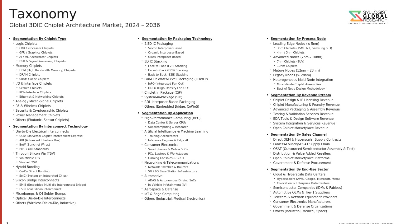
Market Segmentation
- Segmentation By Integration Technology
- Through-Silicon Via (TSV) Based 3D Stacking
- Hybrid Bonding and Direct Bonded Interconnect (DBI)
- Micro-Bump and Controlled Collapse Chip Connection (C4) Integration
- Silicon Interposer and 2.5D Integration (CoWoS and InFO)
- Embedded Multi-Die Interconnect Bridge (EMIB)
- Fan-Out Wafer-Level Package (FOWLP) and Fan-Out Panel-Level Package
- Active Interposer and System-on-Integrated-Chip (SoIC)
- Wafer-on-Wafer (WoW) and Chip-on-Wafer (CoW)
- Others
- Segmentation By Chiplet Interconnect Standard
- Universal Chiplet Interconnect Express (UCIe)
- Bunch of Wires (BoW) and OpenHBI
- Proprietary Die-to-Die Interfaces (TSMC LightSpeed, Intel AIB, and Others)
- High-Bandwidth Memory (HBM) Interface Standards
- Others
- Segmentation By Package Architecture
- 5D Multi-Die on Silicon Interposer
- 3D Stacked Memory-on-Logic
- 3D Stacked Logic-on-Logic
- Multi-Chiplet Fan-Out System-in-Package
- Heterogeneous System-in-Package (SiP) with Mixed Technologies
- Others
- Segmentation By Application
- Artificial Intelligence and Machine Learning Accelerators
- High-Performance Computing (HPC) and Server Processors
- Graphics Processing Units (GPUs) and Visual Computing
- Networking and Data Center Switch ASICs
- Mobile and Consumer Application Processors
- Automotive SoCs and ADAS Processors
- 5G and Telecommunications Infrastructure
- Field-Programmable Gate Arrays (FPGAs) and Adaptive Compute
- Defense, Aerospace, and Space Electronics
- Others
- Segmentation By Component and Supply Chain
- Advanced Packaging Substrates (Silicon Interposers, Organic RDL, and Glass Substrates)
- Through-Silicon Via Formation and Wafer Thinning Equipment
- Hybrid Bonding and Die Attach Equipment
- High-Bandwidth Memory (HBM) Stacked DRAM
- Known-Good-Die Testing and Pre-Bond Screening Infrastructure
- Thermal Interface Materials and Embedded Cooling Solutions
- Electronic Design Automation (EDA) Tools for 3D and Chiplet Design
- Others
- Segmentation By End-User Industry
- Hyperscale Cloud and Data Center Operators
- Semiconductor Integrated Device Manufacturers (IDMs)
- Fabless Semiconductor Companies
- Automotive OEMs and Tier-1 Suppliers
- Telecommunications Equipment Manufacturers
- Defense and Government
- Consumer Electronics Manufacturers
- Others
- Segmentation By Region
- North America
- Europe
- Asia-Pacific
- Middle East and Africa
- Latin America
All market revenues are presented in USD
Historical Year: 2021-2024 | Base Year: 2025 | Estimated Year: 2026 | Forecast Period: 2027-2034
Key Questions this Study Will Answer
- What is the total global market valuation of the 3D IC and Chiplet Architecture Market in the base year 2025, and what is the projected market size and compound annual growth rate through 2034, disaggregated by integration technology including through-silicon via stacking, hybrid bonding, silicon interposer and 2.5D integration, embedded multi-die interconnect bridge, fan-out wafer-level packaging, and active interposer, by application including artificial intelligence accelerators, high-performance computing, graphics processing units, networking ASICs, mobile processors, and automotive SoCs, and by supply chain component including advanced packaging substrates, high-bandwidth memory, known-good-die testing infrastructure, and electronic design automation tools, to enable semiconductor manufacturers, foundries, packaging specialists, hyperscale customers, and capital market investors to identify the highest-growth integration technology and application combinations generating the most commercially durable demand trajectories across the forecast period to 2034?
- How is the transition from monolithic system-on-chip design to chiplet-based heterogeneous integration altering the manufacturing economics, yield curves, process node allocation decisions, and competitive positioning of leading semiconductor companies across artificial intelligence accelerator, server processor, graphics processing unit, and network switch ASIC product categories, and what are the quantified yield improvement, cost per transistor, and system performance metrics that validate chiplet disaggregation economics at different die area, defect density, and process node combinations, and at what die area threshold and process node defect density does chiplet disaggregation deliver superior manufacturing economics relative to monolithic integration for typical high-complexity system-on-chip designs?
- What is the current technology readiness level, production volume, customer adoption status, performance specification, and roadmap trajectory of high-bandwidth memory generations from second generation through fifth generation across SK Hynix, Samsung, and Micron, and how is high-bandwidth memory supply capacity scaling relative to artificial intelligence accelerator demand growth projections through 2034, and what are the technical and manufacturing challenges in high-bandwidth memory fifth generation development including memory stack height, through-silicon via density, power consumption, and yield constraints that could create supply bottlenecks or performance limitations affecting next-generation artificial intelligence training infrastructure procurement timelines and costs?
- What is the current commercial adoption stage, silicon validation coverage, compliance testing infrastructure, and multi-vendor interoperability demonstration status of the Universal Chiplet Interconnect Express standard, and what are the technical specifications, bandwidth tiers, latency characteristics, and power consumption profiles of UCIe compared to proprietary die-to-die interconnect solutions from TSMC, Intel, and AMD, and under what timeline and adoption milestones is UCIe expected to enable a commercially viable multi-vendor chiplet marketplace in which fabless companies can source compute, memory interface, high-speed serial, and analog chiplets from specialized vendors for integration within customer-designed packages without proprietary vendor lock-in, and what structural market changes would a mature open chiplet ecosystem enable across the fabless semiconductor industry?
- How are TSMC, Samsung Foundry, Intel Foundry Services, and leading outsourced semiconductor assembly and test companies including ASE Group and Amkor Technology differentiating their advanced 3D IC and chiplet packaging capabilities across chip-on-wafer-on-substrate, system-on-integrated-chip, foveros, embedded multi-die interconnect bridge, and fan-out wafer-level packaging platforms, what are the capital investment commitments and capacity expansion plans for advanced packaging at each provider through 2034, and how is the strategic migration of the most technically demanding advanced packaging work from outsourced semiconductor assembly and test providers toward front-end foundries with wafer-level hybrid bonding and silicon interposer fabrication capabilities reshaping competitive dynamics, customer relationships, and revenue capture across the advanced semiconductor packaging supply chain?
- Product Definition
- Research Methodology
- Research Design & Framework
- Overall Research Approach: Descriptive, Exploratory & Quantitative Mixed-Method Design
- Market Definition & Scope Boundaries: What is Included and Excluded
- Segmentation Framework
- Key Research Assumptions & Limitations
- Secondary Research
- Primary Research Design & Execution
- Data Triangulation & Validation
- Market Sizing & Forecasting Methodology
- Competitive Intelligence Methodology
- Quality Assurance & Peer Review
- Definitions, Abbreviations & Data Notes
- Research Design & Framework
- Executive Summary
- Market Snapshot & Headline Numbers
- Key Findings & Research Highlights
- Market Dynamics
- Regional Market Summary
- Competitive Landscape Snapshot
- Technology & Innovation Highlights
- Market Dynamics
- Drivers
- Restraints
- Opportunities
- Challenges
- Porter’s Five Forces Analysis
- PESTLE Analysis
- Market Trends & Developments
- Emerging Trends
- Technological Developments
- Regulatory & Policy Changes
- Supply Chain & Sourcing Trends
- Manufacturing & Process Trends
- Investment & Funding Activity
- Sustainability & ESG Trends
- Risk Assessment Framework
- Technology Maturity, Yield Loss & Manufacturability Risk in Advanced 3D Integration
- Geopolitical, Export Control & Semiconductor Supply Chain Concentration Risk
- Chiplet Ecosystem Fragmentation, Interface Standard Incompatibility & IP Boundary Risk
- Thermal Management, Reliability & Long-Term Field Performance Risk
- High Capital Investment, Qualification Cost & Time-to-Market Risk
- Regulatory Framework & Standards
- Semiconductor Export Controls, Entity List Restrictions & Technology Transfer Policy (US EAR, Wassenaar Arrangement, EU Dual-Use Regulation)
- National Semiconductor Industrial Policy & Strategic Autonomy Programmes (US CHIPS Act, EU Chips Act, India Semiconductor Mission, Japan & South Korea Policy)
- Chiplet Open Interface & Interoperability Standards Bodies (UCIe Consortium, OCP, JEDEC, IEEE 3D Integration Standards)
- EDA Tool Control, Advanced Node Lithography (EUV) Equipment Export Restrictions & Foundry Access Policy
- Conflict Mineral, Supply Chain Due Diligence, RoHS, REACH & Environmental Compliance for Advanced Packaging Materials
- Global 3D IC & Chiplet Architecture Market Outlook
- Market Size & Forecast by Value
- Market Size & Forecast by Volume (Units Shipped & Wafer Starts)
- Market Size & Forecast by Integration Technology
- 5D IC Integration via Silicon Interposer (CoWoS, InFO-SoW & Si Interposer Variants)
- 3D IC via Through-Silicon Via (TSV) Stacking
- 3D IC via Hybrid Bonding (Direct Cu-to-Cu, SiO2-SiO2 Dielectric Bonding)
- 3D IC via Wafer-to-Wafer (W2W) Bonding
- 3D IC via Die-to-Wafer (D2W) Bonding
- 3D IC via Die-to-Die (D2D) Bonding
- Chiplet-Based Multi-Die Architecture with Silicon Bridge (EMIB, Foveros Omni, LSI)
- Fan-Out Wafer-Level Package (FOWLP) with Embedded Bridge & RDL Interconnect
- Active Interposer & Reconfigurable Chiplet Platform
- Market Size & Forecast by Interconnect Type
- Through-Silicon Via (TSV) Fine-Pitch Interconnect
- Micro-Bump & Copper Pillar Interconnect
- Direct Copper Hybrid Bonding (Sub-Micron Pitch)
- Silicon Bridge & Embedded Multi-Die Interconnect Bridge (EMIB)
- Redistribution Layer (RDL) & Organic Interposer Interconnect
- Optical & Photonic Interconnect (Emerging Co-Packaged Optics)
- Market Size & Forecast by Chiplet Interface Standard
- UCIe (Universal Chiplet Interconnect Express) Standard
- AIB (Advanced Interface Bus) Open Standard
- BOW (Bunch of Wires) Interface
- OMNI-Link & BoW Derivatives
- Proprietary Chiplet Interface (TSMC CoWoS, Intel EMIB, Samsung X-Cube)
- Market Size & Forecast by Die / Chiplet Function
- Compute & Logic Chiplets (CPU, GPU, NPU & AI Accelerator)
- High-Bandwidth Memory (HBM) & Memory Chiplets (DRAM, SRAM, Flash)
- I/O, SerDes & High-Speed Interface Chiplets
- Analog, Mixed-Signal & RF Chiplets
- Power Management & Integrated Voltage Regulator (IVR) Chiplets
- Security, Encryption & Secure Enclave Chiplets
- Market Size & Forecast by Application
- High-Performance Computing (HPC), Data Centre Server & Cloud Infrastructure
- Artificial Intelligence & Machine Learning Accelerator (Training & Inference)
- Smartphone, Mobile SoC & Consumer Electronics
- Graphics Processing Unit (GPU) & Gaming
- Automotive (ADAS, Central Vehicle Computer, EV Power Domain & In-Cabin AI)
- Networking, Switching & 5G / 6G Base Station
- Industrial Automation, Robotics & Edge AI
- Aerospace, Defence & Space-Grade Electronics
- Market Size & Forecast by End-User
- Integrated Device Manufacturers (IDMs) with In-House Advanced Packaging
- Fabless Semiconductor Design Companies Using Foundry & OSAT Services
- Outsourced Semiconductor Assembly & Test (OSAT) Service Providers
- Cloud Hyperscaler & Data Centre OEMs with Custom Silicon Programmes
- Automotive OEM & Tier-1 Supplier with Custom Chiplet SoC Development
- Government, Defence & National Research Programme Operators
- Market Size & Forecast by Sales Channel
- Foundry & OSAT Direct Contract Supply (TSMC, Samsung, Intel Foundry, ASE, Amkor)
- EDA Software, Process Design Kit (PDK) & Chiplet IP Licensing Channel
- Advanced Packaging Material, Substrate & Bonding Equipment Supply Channel
- Chiplet IP Marketplace & Third-Party Open Chiplet Platform
- North America 3D IC & Chiplet Architecture Market Outlook
- Market Size & Forecast
- By Value
- By Volume (Units Shipped & Wafer Starts)
- By Integration Technology
- By Interconnect Type
- By Chiplet Interface Standard
- By Die / Chiplet Function
- By Application
- By End-User
- By Country
- By Sales Channel
- Market Size & Forecast
- Europe 3D IC & Chiplet Architecture Market Outlook
- Market Size & Forecast
- By Value
- By Volume (Units Shipped & Wafer Starts)
- By Integration Technology
- By Interconnect Type
- By Chiplet Interface Standard
- By Die / Chiplet Function
- By Application
- By End-User
- By Country
- By Sales Channel
- Market Size & Forecast
- Asia-Pacific 3D IC & Chiplet Architecture Market Outlook
- Market Size & Forecast
- By Value
- By Volume (Units Shipped & Wafer Starts)
- By Integration Technology
- By Interconnect Type
- By Chiplet Interface Standard
- By Die / Chiplet Function
- By Application
- By End-User
- By Country
- By Sales Channel
- Market Size & Forecast
- Latin America 3D IC & Chiplet Architecture Market Outlook
- Market Size & Forecast
- By Value
- By Volume (Units Shipped & Wafer Starts)
- By Integration Technology
- By Interconnect Type
- By Chiplet Interface Standard
- By Die / Chiplet Function
- By Application
- By End-User
- By Country
- By Sales Channel
- Market Size & Forecast
- Middle East & Africa 3D IC & Chiplet Architecture Market Outlook
- Market Size & Forecast
- By Value
- By Volume (Units Shipped & Wafer Starts)
- By Integration Technology
- By Interconnect Type
- By Chiplet Interface Standard
- By Die / Chiplet Function
- By Application
- By End-User
- By Country
- By Sales Channel
- Market Size & Forecast
- Country-Wise* 3D IC & Chiplet Architecture Market Outlook
- Market Size & Forecast
- By Value
- By Volume (Units Shipped & Wafer Starts)
- By Integration Technology
- By Interconnect Type
- By Chiplet Interface Standard
- By Die / Chiplet Function
- By Application
- By End-User
- By Country
- By Sales Channel
- Market Size & Forecast
*Countries Analyzed in the Syllogist Global Research Portfolio: United States, Canada, Germany, France, United Kingdom, Netherlands, Belgium, Sweden, Switzerland, Japan, South Korea, Taiwan, China, Singapore, Malaysia, India, Israel, Australia, Brazil, UAE, Saudi Arabia, Vietnam, Thailand
- Technology Landscape & Innovation Analysis
- Through-Silicon Via (TSV) Fabrication & 3D Stacking Technology Deep-Dive
- Hybrid Bonding & Direct Copper-to-Copper Sub-Micron Interconnect Technology
- Chiplet Interface, Interoperability & UCIe Open Standard Ecosystem Technology
- 5D Silicon Interposer, Silicon Bridge & Embedded Interconnect Technology
- Wafer-to-Wafer & Die-to-Wafer Bonding Process & Alignment Technology
- High-Bandwidth Memory (HBM) Stacking, 3D DRAM & Near-Memory Computing Technology
- Thermal Management, Heat Dissipation & Reliability Testing Technology for 3D IC and Chiplet Assemblies
- EDA Co-Design, Simulation, Known-Good-Die (KGD) Test & System-Level Verification Technology
- Patent & IP Landscape in 3D IC & Chiplet Architecture
- Value Chain & Supply Chain Analysis
- Silicon Wafer, Substrate, Bonding Material & Advanced Dielectric Supply Chain
- Lithography, Etch, CMP, Deposition & TSV Process Equipment Supply Chain
- Advanced Packaging Equipment, Bonder, Flip-Chip & OSAT Process Tool Supply Chain
- EDA Software, Process Design Kit (PDK), IP Core & Chiplet IP Provider Landscape
- Foundry, OSAT & Integrated Device Manufacturer (IDM) Service Provider Landscape
- Systems OEM, Cloud Hyperscaler & End-Market Customer Integration Channel
- Test, Inspection, Known-Good-Die (KGD) Qualification & Yield Management
- Pricing Analysis
- 5D CoWoS & Silicon Interposer Packaging Cost vs. Monolithic SoC Benchmark Analysis
- 3D IC TSV Stacking & Hybrid Bonding Advanced Packaging Cost Analysis
- Chiplet-Based Multi-Die SoC Total Cost vs. Equivalent Monolithic SoC Analysis
- HBM Memory Stack Pricing & Cost Trajectory Analysis
- OSAT Advanced Packaging Service Pricing by Technology Node & Complexity
- Total System Cost Optimisation: Chiplet Disaggregation Economics, Yield Improvement Benefit & Time-to-Market Value Analysis
- Sustainability & Environmental Analysis
- Lifecycle Assessment (LCA) of 3D IC & Chiplet Architecture vs. Monolithic SoC: Carbon Footprint, Water Consumption & Energy Intensity Comparison
- Die Disaggregation & Chiplet Reuse: Sustainability Benefit of Node-Optimised Chiplets and Reduced Semiconductor Waste from Yield-Limited Monolithic Devices
- Advanced Packaging Material Sustainability: Lead-Free Solder, Halogen-Free Substrate & Low-CTE Underfill Compliance with RoHS, REACH & Green Electronics Standards
- Semiconductor Fab Water Usage, Chemical Waste & Energy Intensity of 3D Integration Process Steps
- Regulatory-Driven Sustainability: US CHIPS Act Environmental Provisions, EU Green Electronics Policy & SDG Alignment for Advanced Semiconductor Manufacturing
- Competitive Landscape
- Market Structure & Concentration
- Market Consolidation Level (Fragmented vs. Consolidated by Integration Technology & Geography)
- Top 10 Players Market Share
- HHI (Herfindahl-Hirschman Index) Concentration Analysis
- Competitive Intensity Map by Integration Technology, Application & Geography
- Player Classification
- Leading Foundries with Advanced 3D IC & Chiplet Integration Capability (TSMC, Samsung Foundry, Intel Foundry)
- Integrated Device Manufacturers (IDMs) with Proprietary 3D Integration Platforms
- Outsourced Semiconductor Assembly & Test (OSAT) Providers with Advanced Packaging Capability
- Fabless Chiplet Architecture Pioneers & Multi-Die SoC Design Companies
- EDA Software, Chiplet IP & Process Design Kit (PDK) Providers
- Advanced Packaging Material, Substrate & Bonding Chemical Suppliers
- Test, Inspection & Known-Good-Die (KGD) Equipment & Service Providers
- Chiplet IP Marketplace & Open Ecosystem Platform Companies
- Competitive Analysis Frameworks
- Market Share Analysis by Integration Technology, Application & Region
- Company Profile
- Company Overview & Headquarters
- 3D IC & Chiplet Products, Services & Technology Portfolio
- Key Customer Relationships & Design-Win Reference Projects
- Manufacturing Footprint, Fab & OSAT Capacity
- Revenue (3D IC & Chiplet Segment) & Backlog
- Technology Differentiators & IP
- Key Strategic Partnerships, JVs & M&A Activity
- Recent Developments (Capacity Expansion, Product Launches, Customer Wins)
- SWOT Analysis
- Strategic Focus Areas & Roadmap
- Competitive Positioning Map (Technology Capability vs. Market Penetration)
- Key Company Profiles
- Market Structure & Concentration
- Technology Landscape & Innovation Analysis
- Strategic Output
- Market Opportunity Matrix: By Integration Technology, Chiplet Function, Application, End-User & Geography
- White Space Opportunity Analysis
- Strategic Output
- Strategic Recommendations
- Product Portfolio & Technology Investment Strategy
- Manufacturing & Operational Excellence Strategy
- Geographic Expansion & Localisation Strategy
- Customer & OEM Engagement Strategy
- Partnership, M&A & Ecosystem Strategy
- Sustainability & Circular Economy Strategy
- Risk Mitigation & Future Roadmap
- Strategic Priority Matrix & Roadmap
- Near-term (2025-2028)
- Mid-term (2029-2032)
- Long-term (2033-2037)