Market Definition
The Global Advanced Semiconductor Packaging Market encompasses the engineering, manufacturing, and supply of sophisticated assembly and interconnection technologies that house, protect, electrically connect, and thermally manage integrated circuit dies within package structures whose dimensional, electrical, and thermal performance specifications are critical determinants of end semiconductor device performance in artificial intelligence accelerators, high-performance computing processors, mobile system-on-chips, high-bandwidth memory stacks, power devices, radio frequency components, and optoelectronic modules. Advanced packaging distinguishes itself from conventional wire bond and lead frame packaging through the utilisation of fine-pitch interconnect technologies, three-dimensional die stacking architectures, wafer-level processing techniques, and heterogeneous integration capabilities that enable the co-packaging of multiple dies from different process nodes, material systems, and functional domains within a single package footprint, achieving system-level performance, bandwidth, and power efficiency outcomes that monolithic die scaling alone cannot deliver at economically viable yields as semiconductor process geometries approach fundamental physical limits. The technology scope of the market includes flip chip packaging with solder bump or copper pillar interconnects, wafer-level chip scale packaging, fan-out wafer-level and panel-level packaging, two-dimensional and three-dimensional chip-on-wafer-on-substrate and chip-on-wafer configurations, through-silicon via-enabled three-dimensional integrated circuits and high-bandwidth memory stacks, silicon interposer and organic substrate-based 2.5D integration platforms, embedded die packaging, system-in-package multi-chip modules, and the glass and silicon bridge chiplet interconnect architectures enabling disaggregated semiconductor design. The market value chain encompasses substrate and interposer manufacturers, packaging material and chemical suppliers, assembly and test service providers, advanced packaging equipment manufacturers, electronic design automation tool vendors, and the integrated device manufacturers, fabless semiconductor companies, and outsourced semiconductor assembly and test service operators whose system performance, cost, and time-to-market requirements define the advanced packaging technology adoption trajectory globally.
Market Insights
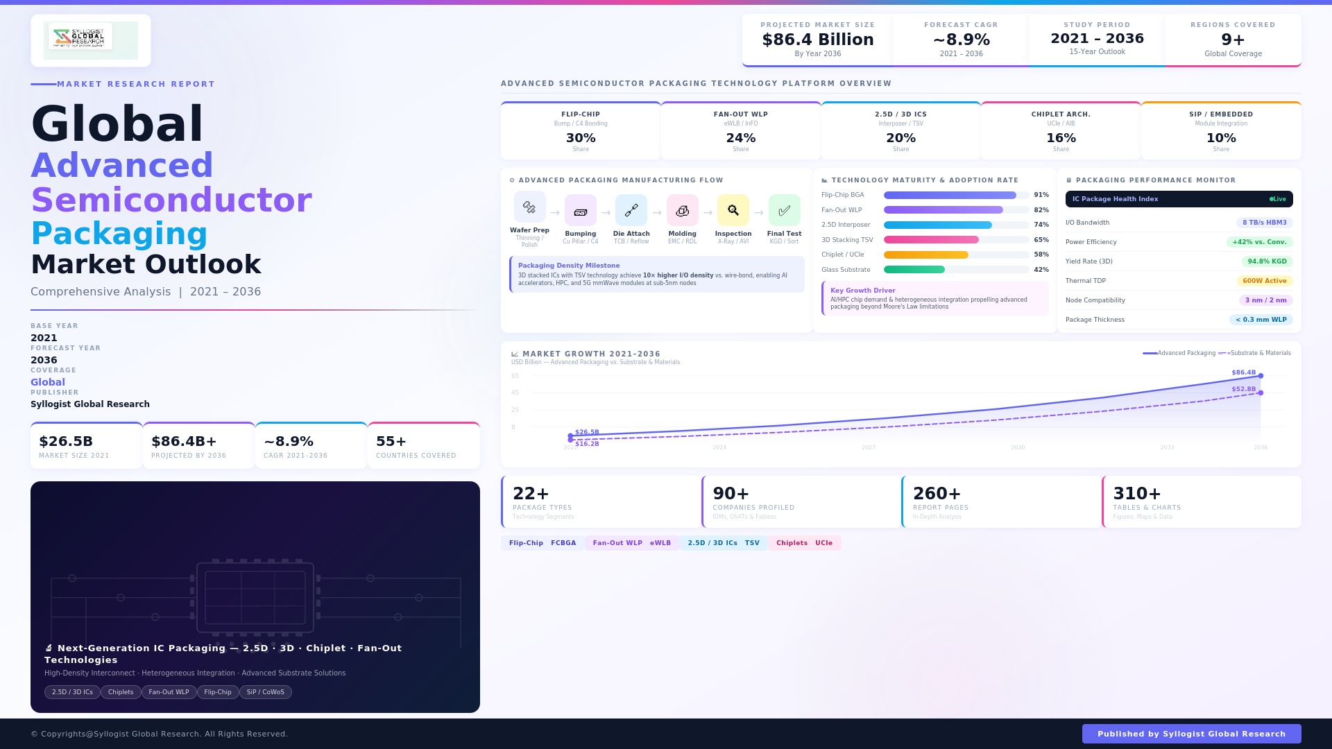
The global advanced semiconductor packaging market was valued at approximately USD 42.8 billion in 2025 and is projected to reach USD 98.6 billion by 2034, advancing at a compound annual growth rate of 9.7% over the forecast period from 2027 to 2034, driven by the structural transition of the semiconductor industry toward heterogeneous integration as the primary vehicle for continued system performance scaling beyond the limitations of traditional monolithic die lithographic node advancement, with artificial intelligence workload requirements for high-bandwidth memory and processor integration creating a concentrated near-term demand catalyst whose commercial scale is expanding the advanced packaging market at a pace substantially exceeding that of the broader semiconductor industry. The convergence of artificial intelligence compute demand, the physical and economic limits of transistor density scaling at leading-edge nodes, and the system architect preference for integrating best-in-class dies from different foundries and process nodes within optimised package configurations is creating a structural and durable transition of semiconductor system design philosophy toward packaging-centric architecture that is fundamentally revaluing the strategic importance and technology complexity of the packaging layer within the semiconductor value chain.
The artificial intelligence accelerator and high-performance computing segment is the most commercially significant demand driver for advanced packaging technology, with large-scale AI training and inference chips incorporating high-bandwidth memory stacks connected through through-silicon via three-dimensional integration, and multiple compute chiplets interconnected through silicon interposer or organic substrate 2.5D platforms at packaging densities and interconnect bandwidths that fundamentally determine the performance and power efficiency of the complete AI accelerator system. A single advanced AI accelerator package incorporating silicon interposer 2.5D integration with eight high-bandwidth memory stacks represents a packaging bill of materials value of approximately USD 400 to USD 900 per unit depending on package configuration, interposer size, and memory stack count, compared to conventional flip chip package values of USD 15 to USD 80 per unit for comparable die counts, illustrating the order-of-magnitude uplift in packaging value intensity that advanced heterogeneous integration platforms deliver relative to conventional packaging approaches. Fan-out packaging technology, encompassing both wafer-level and panel-level format variants, is growing at approximately 14.2% annually across mobile application processor, power management integrated circuit, radio frequency module, and automotive radar packaging applications where the combination of fine-pitch die-to-die and die-to-package substrate routing capability, thin form factor, and elimination of conventional organic substrates delivers density, cost, and performance advantages that are making fan-out the dominant packaging format for advanced mobile and automotive semiconductor applications at leading-edge foundries and outsourced semiconductor assembly and test operators globally.
Taiwan occupies a uniquely central and strategically indispensable position within the global advanced semiconductor packaging ecosystem, with Taiwan Semiconductor Manufacturing Company’s integrated foundry-plus-advanced-packaging offering combining leading-edge silicon fabrication with chip-on-wafer-on-substrate, system-on-integrated-chips, and three-dimensional fabric stacking packaging platforms in a single supply chain relationship that enables semiconductor designers to access co-optimised front-end and back-end processes whose tight integration is essential for achieving the interconnect density and signal integrity performance of the most advanced heterogeneous integration packages. The geographic concentration of advanced packaging capacity in Taiwan, South Korea, and China, which collectively account for approximately 78% of global outsourced semiconductor assembly and test revenue in 2025, has prompted semiconductor supply chain security concerns among American, European, and Japanese governments and semiconductor companies whose critical system applications in defence, automotive, telecommunications, and computing infrastructure require assured access to advanced packaging capability outside of potentially vulnerable concentrated geographic supply regions. The United States CHIPS and Science Act is investing approximately USD 2.8 billion in advanced packaging research, development, and manufacturing facility establishment through the National Advanced Packaging Manufacturing Program, while similar advanced packaging localisation investments are underway in Japan through the Rapidus partnership with leading foundry technology, the European Chips Act programs supporting advanced packaging facility development at Infineon, STMicroelectronics, and other European semiconductor manufacturers, and Intel’s advanced packaging capacity expansion programs at facilities in Arizona, New Mexico, and Ireland that collectively represent a multi-year structural shift in advanced packaging geographic capacity distribution.
Chiplet architecture and disaggregated semiconductor design represent the most structurally significant long-term market development within the advanced packaging industry, with the transition from monolithic die design toward modular chiplet-based system assembly enabling semiconductor companies to combine processing, memory, input-output, and analog dies from different foundries, process nodes, and geographic manufacturing sources within a single package, reducing development risk and time-to-market while optimising cost and performance across individual functional die types that can be independently sourced, validated, and reused across multiple product generations. The Universal Chiplet Interconnect Express specification, the Open Compute Project Advanced Packaging work group standards, and equivalent industry-driven interconnect standardisation initiatives are progressively establishing the die-to-die interface standards whose wide adoption will enable a multi-vendor chiplet supply ecosystem analogous to the printed circuit board component ecosystem, with chiplet marketplace platforms already emerging as commercial entities offering catalogued intellectual property validated chiplet dies available for system-in-package integration by fabless semiconductor designers who do not operate their own silicon fabrication capability. Thermal management has emerged as a critical and commercially significant technical challenge in advanced packaging, with three-dimensional die stacking and high-density heterogeneous integration architectures generating thermal flux densities of 100 to 300 watts per square centimetre at the package level that conventional heat spreader and thermal interface material approaches are insufficient to manage within the junction temperature limits of stacked dies, driving investment in advanced thermal interface materials, microchannel liquid cooling integration within package structures, thermoelectric cooling elements, and vapour chamber spreading solutions that constitute a growing and technically sophisticated ancillary market within the broader advanced packaging ecosystem.
Key Drivers
Artificial Intelligence Accelerator Demand and High-Bandwidth Memory Integration Requirements Creating Historically Unprecedented Advanced Packaging Technology Adoption and Value Intensity Growth
The exponential growth of artificial intelligence training and inference workloads is generating a demand trajectory for advanced semiconductor packages that integrate the highest-bandwidth memory stacks and the densest chiplet interconnect architectures commercially available, creating a concentrated and high-value demand catalyst for silicon interposer 2.5D integration, through-silicon via three-dimensional high-bandwidth memory stacking, and chip-on-wafer-on-substrate heterogeneous integration platforms whose packaging value intensity per completed system is an order of magnitude above that of conventional semiconductor packaging applications. Global artificial intelligence accelerator chip revenue reached approximately USD 67 billion in 2025 and is projected to exceed USD 180 billion by 2034, with advanced packaging representing approximately 18% to 25% of total accelerator system cost depending on memory bandwidth configuration and die count, creating a direct advanced packaging market demand stream whose scale and growth rate are driving capacity investment across silicon interposer fabrication, high-bandwidth memory wafer bonding, and organic substrate manufacturing at a pace that strains the existing supply chain capacity of the most technically demanding packaging process steps. The hyperscale data centre operators deploying AI accelerator clusters at scale of tens of thousands to hundreds of thousands of units per facility are creating procurement volumes for advanced packaged AI chips that are driving foundry and packaging service providers to commit to multi-year capacity expansion programs whose scale and capital intensity are transforming the business model economics of advanced packaging from custom engineering engagement to high-volume manufacturing operation, with annual capital expenditure commitments for advanced packaging capacity expansion across leading packaging service providers exceeding USD 8 billion collectively in 2025.
Physical Limits of Monolithic Die Scaling and Economic Constraints of Leading-Edge Node Fabrication Compelling Heterogeneous Integration as the Primary System Performance Scaling Vehicle
The progressive slowdown of transistor density scaling improvement per process node generation, combined with the exponentially increasing capital cost of leading-edge wafer fabrication at 3-nanometer and 2-nanometer nodes where a single advanced logic fab represents USD 20 billion to USD 30 billion in construction and equipment investment, is compelling semiconductor system architects to pursue performance, bandwidth, and power efficiency improvement through packaging architecture innovation rather than relying exclusively on lithographic node advancement whose cost-performance improvement trajectory has become significantly less favourable than the historical pace of Moore’s Law scaling from which semiconductor industry economics have historically been derived. The economics of heterogeneous integration, which allow different dies to be manufactured at their respective optimal process nodes and assembled into a single high-performance package rather than attempting to integrate all functions on a single die at the most advanced available node, are generating substantial cost and yield advantages in applications where mixing logic at 3-nanometer, memory at mature nodes, and analog or radio frequency functions at specialty process nodes produces better system performance per dollar than any monolithic integration approach could achieve. Leading semiconductor designers including artificial intelligence chip companies, graphics processor developers, and data centre central processing unit architects have formally committed to chiplet-based design strategies for their next-generation product families, with publicly announced roadmaps specifying heterogeneous integration package architectures for products entering sampling in 2026 and 2027 that will collectively generate advanced packaging demand across silicon interposer, fan-out, and three-dimensional wafer bonding technology categories at volumes substantially larger than current commercial production.
Automotive Semiconductor Electrification and Advanced Driver Assistance System Content Growth Driving Advanced Packaging Adoption in High-Reliability Vehicle Applications
The electrification of vehicle powertrains and the proliferation of advanced driver assistance systems and autonomous driving sensor processing platforms are generating rapidly expanding demand for advanced semiconductor packages qualified for automotive operating environments, where the combination of elevated temperature cycling, vibration, humidity exposure, and functional safety requirements imposes packaging qualification standards substantially more demanding than those applicable to consumer or industrial semiconductor applications, and where the system performance requirements of multi-gigabit radar and camera signal processing, high-voltage power switching, and battery management computing are driving adoption of advanced packaging technologies previously confined to high-performance computing applications. Electric vehicle power inverter modules incorporating silicon carbide power dies in advanced multi-chip power module configurations are growing at approximately 22.6% annually, driven by the superior switching efficiency and thermal performance of advanced packaged silicon carbide relative to discrete silicon power packaging in high-voltage battery-to-motor conversion applications, with the average advanced packaging content per battery electric vehicle power conversion system reaching approximately USD 280 to USD 420 per vehicle depending on drive train configuration and silicon carbide die count. Automotive system-on-chip packages for advanced driver assistance system domain controllers are incorporating fan-out system-in-package and chiplet integration approaches that combine application processor, memory, and connectivity dies in packages qualified to automotive grade one temperature and reliability standards, with each advanced driver assistance system domain controller representing a packaging bill of materials of USD 45 to USD 120 per vehicle, generating a growing and technically demanding automotive advanced packaging revenue stream that is less cyclical and more resilient than the consumer electronics packaging demand that has historically dominated outsourced semiconductor assembly and test revenue.
Key Challenges
Extreme Capital Intensity of Advanced Packaging Capacity Investment, Long Equipment Lead Times, and Yield Ramp Challenges at Novel Integration Process Steps
The capital intensity of building advanced semiconductor packaging capacity at the process capability levels required for silicon interposer fabrication, through-silicon via formation, hybrid wafer bonding, and fine-pitch copper pillar flip chip assembly is approaching the capital requirements of wafer fabrication itself, with a state-of-the-art advanced packaging facility capable of volume production of silicon interposer-based 2.5D packages representing a capital investment of USD 3 billion to USD 7 billion including cleanroom infrastructure, lithographic and etch equipment for interposer patterning, wafer bonding tools, and the advanced inspection and metrology systems required to maintain yield at interconnect pitches below 10 micrometres. Equipment lead times for critical advanced packaging process tools including thermocompression bonding systems, wafer bonders for hybrid bonding and three-dimensional stacking, and advanced lithography systems for interposer and redistribution layer patterning extend to 18 to 30 months from order placement to installation qualification, creating supply chain rigidity that prevents rapid capacity scaling in response to demand acceleration and generates structural supply constraints at peak advanced packaging demand periods whose resolution requires capital commitment decisions made 24 to 36 months before the revenue that justifies them is realized. Yield management at novel advanced packaging process steps presents persistent technical challenges, with copper pillar bump bridging defects, underfill voiding in fine-pitch flip chip assemblies, through-silicon via resistance variation in three-dimensional stacked dies, and hybrid bonding copper surface roughness and contamination sensitivity all requiring sustained process engineering investment to achieve the yield levels necessary for economically viable high-volume manufacturing of the most advanced package configurations.
Supply Chain Concentration and Geopolitical Risk in Advanced Substrate, Interposer, and Specialty Packaging Material Supply Chains
The advanced semiconductor packaging supply chain exhibits extreme geographic concentration at multiple critical material and process steps whose disruption could cascade rapidly through the global semiconductor supply chain to affect the availability of artificial intelligence accelerators, mobile processors, automotive microcontrollers, and other advanced packaged devices whose uninterrupted supply is critical to the functioning of digitally dependent global industries. Advanced organic substrates for flip chip and fan-out packages are produced by a small number of Japanese, South Korean, and Taiwanese substrate manufacturers whose combined capacity is constrained by the capital and process technology barriers to new entrant development, with substrate supply tightness during peak demand periods having been identified as a primary constraint on semiconductor output growth in recent industry cycles, and with the geographic concentration of substrate capacity creating single-region supply vulnerability to natural disaster, geopolitical disruption, or pandemic-related manufacturing interruption. Silicon interposer fabrication, whose process technology requirements are comparable to front-end semiconductor wafer processing at 65-nanometer to 130-nanometer design rules, is performed almost exclusively by Taiwan Semiconductor Manufacturing Company and a small number of Asian outsourced semiconductor assembly and test operators, with the geographic concentration of this capability in Taiwan representing a geopolitical supply risk that semiconductor companies and governments are investing to diversify through domestic interposer capacity development programs in the United States, Japan, and Europe whose commercial production timelines extend beyond 2027 and whose initial capacity will represent only a small fraction of global demand.
Thermal Management Complexity, Power Density Escalation, and Coefficient of Thermal Expansion Mismatch Reliability Challenges in Three-Dimensional and High-Density Heterogeneous Integration Packages
The progressive increase in power density within advanced semiconductor packages, driven by the aggregation of multiple high-performance compute and memory dies within increasingly compact package footprints whose thermal dissipation path to external heat sinking is constrained by the mechanical and material architecture of the package structure, is creating thermal management challenges at three-dimensional integrated and 2.5D heterogeneous packages that are emerging as one of the primary technical constraints on the maximum performance achievable within package thermal budget limitations, requiring innovation in thermal interface materials, package-integrated cooling structures, and system-level thermal co-design methodologies that extend well beyond the conventional heat spreader and thermal compound approaches adequate for prior-generation packages. The coefficient of thermal expansion mismatch between silicon dies, silicon or glass interposers, organic laminate substrates, and copper metallisation at the thermal cycling conditions experienced during package assembly reflow and end product operation generates thermomechanical stress at solder interconnects, underfill interfaces, and through-silicon via structures whose cumulative fatigue damage over product service life must be managed within reliability qualification standards including joint electron device engineering council standards for automotive and high-reliability applications, requiring package architects to optimise interconnect design, underfill material selection, and warpage control across the complete package stack in co-simulation environments whose computational requirements are substantially greater than those needed for conventional package reliability prediction. The integration of liquid cooling channels and thermoelectric elements within advanced package structures to manage thermal flux densities exceeding 100 watts per square centimetre represents an active area of development whose commercial productisation at volume is constrained by manufacturing complexity, cost, and reliability validation requirements that are not yet fully resolved at the process maturity levels required for high-volume semiconductor manufacturing.
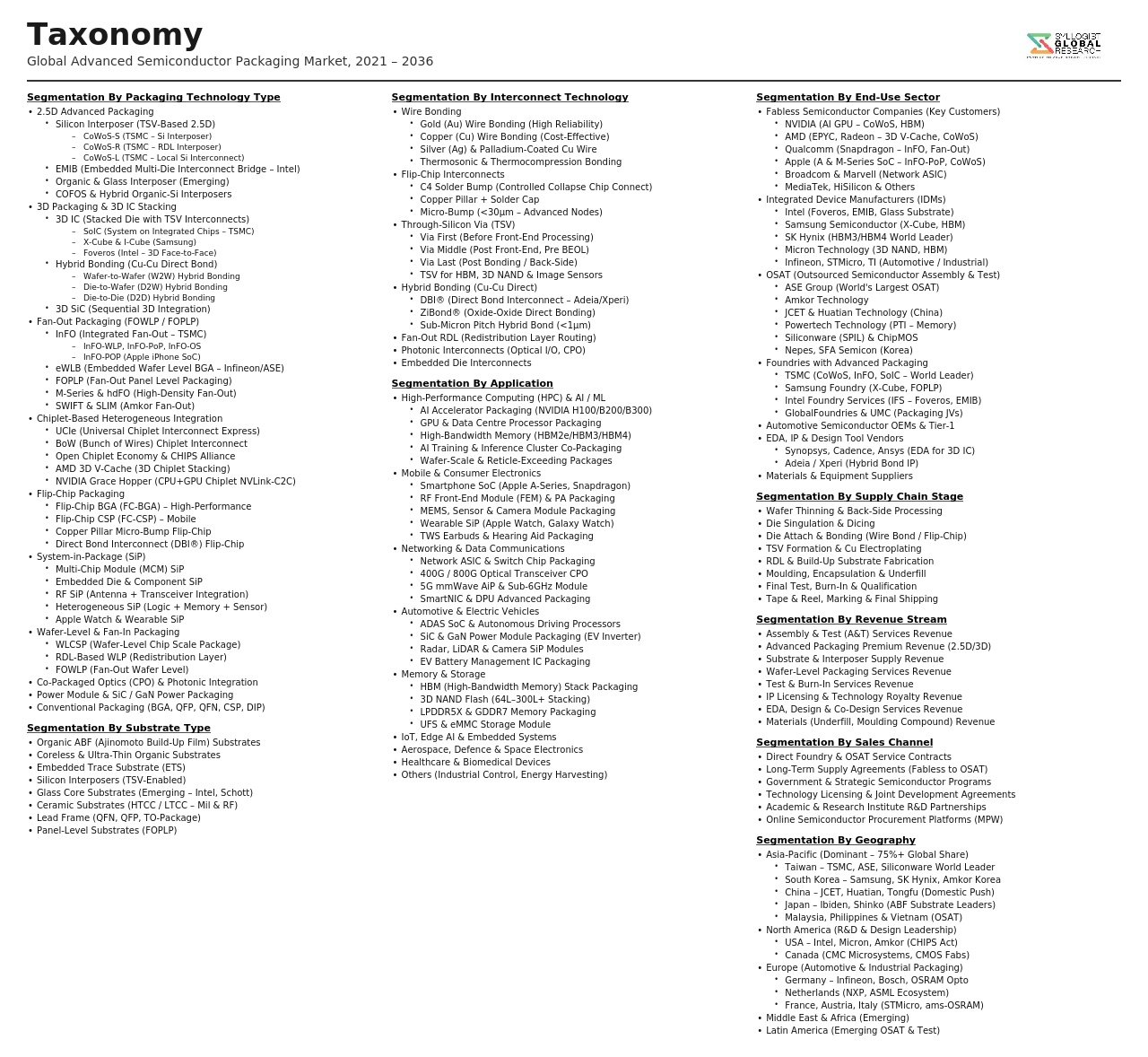
Market Segmentation
- Segmentation By Packaging Technology
- Flip Chip with Copper Pillar and Solder Bump Interconnects
- Fan-Out Wafer-Level Packaging (FO-WLP)
- Fan-Out Panel-Level Packaging (FO-PLP)
- Wafer-Level Chip Scale Packaging (WLCSP)
- Silicon Interposer 2.5D Integration (CoWoS and Equivalent)
- Through-Silicon Via (TSV) Three-Dimensional Stacking
- Hybrid Bonding and Direct Copper-to-Copper Interconnect
- System-in-Package (SiP) Multi-Chip Modules
- Embedded Die Packaging
- Glass Substrate and Glass Core Packaging
- Others
- Segmentation By Integration Architecture
- Two-Dimensional Multi-Chip Module (2D MCM)
- 5D Integration with Interposer or Bridge
- Three-Dimensional Stacked Integrated Circuits (3D-IC)
- Three-Dimensional High-Bandwidth Memory (HBM) Stacks
- Heterogeneous Chiplet Integration
- Monolithic Advanced Single-Die Packaging
- Segmentation By End-Use Application
- Artificial Intelligence Training and Inference Accelerators
- High-Performance Computing (HPC) Processors and GPUs
- Mobile Application Processors and System-on-Chips
- High-Bandwidth Memory (HBM) for AI and HPC
- Networking and Data Centre Switch ASICs
- Automotive ADAS and Domain Controller Processors
- Automotive Power Modules (Silicon Carbide and GaN)
- Radio Frequency and Millimetre-Wave Modules
- Consumer Electronics and Wearables
- Others
- Segmentation By Service Model
- Outsourced Semiconductor Assembly and Test (OSAT) Services
- Integrated Device Manufacturer (IDM) Captive Packaging
- Foundry-Integrated Advanced Packaging (Foundry-OSAT)
- Substrate and Interposer Manufacturing Services
- Advanced Packaging Equipment and Materials Supply
- Segmentation By Substrate Type
- Organic Laminate Substrates (ABF and BT Resin)
- Silicon Interposers
- Glass Core and Glass Interposer Substrates
- Ceramic Substrates
- Flexible and Embedded Substrates
- Others
- Segmentation By Interconnect Technology
- Solder Bump (C4 and Micro-Bump) Flip Chip
- Copper Pillar Flip Chip
- Through-Silicon Via (TSV) Interconnects
- Hybrid Bonding (Direct Copper-to-Copper)
- Redistribution Layer (RDL) Fine-Pitch Routing
- Die-to-Die Bridge Interconnects (EMIB and Foveros)
- Segmentation By End Device
- Data Centre Servers and AI Compute Systems
- Smartphones and Mobile Devices
- Automotive Systems (EV, ADAS, and Infotainment)
- Personal Computers and Workstations
- Network Infrastructure Equipment
- Industrial and Medical Electronics
- Aerospace and Defence Systems
- Segmentation By Region
- Asia-Pacific (Taiwan, South Korea, China, Japan, and Others)
- North America (United States)
- Europe (Germany, Ireland, Netherlands, and Others)
- Rest of World
All market revenues are presented in USD
Historical Year: 2021-2024 | Base Year: 2025 | Estimated Year: 2026 | Forecast Period: 2027-2034
Key Questions this Study Will Answer
- What is the total global market valuation of the Advanced Semiconductor Packaging Market in the base year 2025, and what is the projected market size and compound annual growth rate through 2034, disaggregated by packaging technology, silicon interposer 2.5D, through-silicon via 3D stacking, fan-out wafer-level and panel-level, flip chip, and system-in-package, by end-use application, artificial intelligence and HPC, mobile, automotive, and networking, and by service model, integrated device manufacturer captive and outsourced semiconductor assembly and test, to enable packaging service providers, equipment manufacturers, materials suppliers, semiconductor designers, and investors to identify which technology platforms and end-use markets will generate the highest absolute revenue and most commercially significant adoption momentum across the forecast period?
- How is the artificial intelligence accelerator and high-bandwidth memory integration market expected to drive advanced packaging technology investment, capacity expansion, and competitive positioning through 2034, what are the projected silicon interposer, organic substrate, and wafer bonding capacity requirements associated with anticipated AI chip production volumes, which packaging service providers and substrate manufacturers are best positioned to capture the advanced packaging content uplift from AI accelerator demand growth, and how are hyperscale data centre operator procurement volumes and long-term supply agreements reshaping the business model economics and capital investment planning of the advanced semiconductor packaging industry?
- What is the commercial trajectory of chiplet architecture adoption and the Universal Chiplet Interconnect Express and equivalent die-to-die interface standardisation initiatives through 2034, which semiconductor end markets and product categories are generating the most significant near-term chiplet design activity, how are multi-vendor chiplet supply ecosystem development and chiplet marketplace platform emergence expected to reshape the value chain economics and competitive dynamics of advanced packaging service providers, and what are the technical requirements in terms of interconnect pitch, bandwidth density, and power efficiency that advanced packaging platforms must achieve to serve the most demanding chiplet integration applications across artificial intelligence, high-performance computing, and automotive domains?
- How are the United States CHIPS Act National Advanced Packaging Manufacturing Program, Japan Rapidus and advanced packaging capacity investment programs, European Chips Act advanced packaging facility support, and Intel advanced packaging capacity expansion at US and European sites expected to shift the geographic distribution of advanced packaging capacity and supply chain resilience through 2034, what are the technical capability gaps that new ex-Asia advanced packaging capacity must close relative to established Taiwan and South Korea-based capabilities, and what are the implications for semiconductor companies designing advanced packaging-dependent products for end markets with supply chain localisation requirements?
- Who are the leading outsourced semiconductor assembly and test providers, integrated device manufacturers with captive advanced packaging operations, silicon interposer and organic substrate manufacturers, advanced packaging equipment suppliers, and specialty packaging material developers currently defining the competitive landscape of the global advanced semiconductor packaging market, and what are their respective technology platform coverage across packaging architectures and interconnect generations, capital expenditure programs and capacity expansion timelines, research and development investment in hybrid bonding and panel-level packaging technologies, customer program engagement with leading artificial intelligence chip designers, and competitive positioning responses to the thermal management, supply chain concentration, and yield ramp challenges reshaping advanced packaging competitive dynamics through 2034?
- Product Definition
- Research Methodology
- Research Design & Framework
- Overall Research Approach: Descriptive, Exploratory & Quantitative Mixed-Method Design
- Market Definition & Scope Boundaries: What is Included and Excluded
- Segmentation Framework
- Key Research Assumptions & Limitations
- Secondary Research
- Primary Research Design & Execution
- Data Triangulation & Validation
- Market Sizing & Forecasting Methodology
- Competitive Intelligence Methodology
- Quality Assurance & Peer Review
- Definitions, Abbreviations & Data Notes
- Research Design & Framework
- Executive Summary
- Market Snapshot & Headline Numbers
- Key Findings & Research Highlights
- Market Dynamics
- Regional Market Summary
- Competitive Landscape Snapshot
- Technology & Innovation Highlights
- Market Dynamics
- Drivers
- Restraints
- Opportunities
- Challenges
- Porter’s Five Forces Analysis
- PESTLE Analysis
- Market Trends & Developments
- Emerging Trends
- Technological Developments
- Regulatory & Policy Changes
- Supply Chain & Sourcing Trends
- Manufacturing & Process Trends
- Investment & Funding Activity
- Sustainability & ESG Trends
- Risk Assessment Framework
- Geopolitical, Export Control & Supply Chain Concentration Risk in Semiconductor Packaging
- Technology Transition, Node Shrink & Packaging Complexity Execution Risk
- Substrate, Advanced Material & Critical Chemical Supply Shortage Risk
- Capital Intensity, Yield Ramp & Return on Investment Risk for Advanced Packaging Fabs
- Intellectual Property, Standards Fragmentation & Ecosystem Lock-In Risk
- Regulatory Framework & Standards
- Export Controls, Trade Restrictions & National Security Regulations Impacting Advanced Semiconductor Packaging
- JEDEC, IPC & Industry Packaging Standards, Reliability Testing & Qualification Requirements
- Environmental Regulations: RoHS, REACH, Hazardous Substance Restrictions & Green Chemistry Standards
- Government Incentive Programmes, Fab Investment Subsidies & Domestic Semiconductor Manufacturing Policy
- Sustainability, Carbon Footprint Disclosure & ESG Reporting Standards for Semiconductor Manufacturing
- Global Advanced Semiconductor Packaging Market Outlook
- Market Size & Forecast by Value
- Market Size & Forecast by Volume (Units)
- Market Size & Forecast by Package Type
- 5D Packaging (Interposer-Based & Silicon Bridge)
- 3D Packaging (3D IC Stacking & 3D NAND)
- Fan-Out Wafer-Level Packaging (FOWLP)
- Fan-In Wafer-Level Packaging (FIWLP)
- Flip Chip Ball Grid Array (FC-BGA)
- Flip Chip Chip-Scale Package (FC-CSP)
- System-in-Package (SiP)
- Chiplet-Based Multi-Die Packaging
- Embedded Die & Panel-Level Packaging
- Other Advanced Package Formats
- Market Size & Forecast by Technology
- Through-Silicon Via (TSV) Technology
- Copper Pillar Bumping & Micro-Bump Interconnect Technology
- Hybrid Bonding & Direct Bonding Interconnect (DBI) Technology
- Redistribution Layer (RDL) & Fine-Line Interposer Technology
- Wafer-Level Moulding & Reconstitution Technology
- Laser Ablation, Lithography & Advanced Patterning Technology
- Thermal Interface Material (TIM) & Advanced Thermal Management Technology
- Market Size & Forecast by Substrate Type
- Organic Substrate (ABF, BT Resin)
- Silicon Interposer
- Glass Interposer
- Ceramic Substrate
- Embedded Trace Substrate (ETS)
- Panel-Level Substrate
- Market Size & Forecast by End-Use Industry
- Consumer Electronics (Smartphones, Tablets & Wearables)
- Data Centre, Cloud Computing & High-Performance Computing (HPC)
- Artificial Intelligence & Machine Learning Accelerators
- Automotive (ADAS, EV Power Electronics & In-Vehicle Networking)
- 5G & Telecommunications Infrastructure
- Industrial Automation & IoT
- Aerospace & Defence
- Healthcare & Medical Devices
- Market Size & Forecast by Application
- Processors & Application-Specific Integrated Circuits (ASICs)
- Memory (DRAM, HBM & 3D NAND Flash)
- Power Management Integrated Circuits (PMICs)
- Radio Frequency (RF) & Millimetre Wave (mmWave) Devices
- Image Sensors & Optical Devices
- MEMS & Sensor Packages
- Market Size & Forecast by Sales Channel
- Outsourced Semiconductor Assembly & Test (OSAT) Providers
- Integrated Device Manufacturers (IDMs) with In-House Packaging
- Foundry-Led Advanced Packaging Services
- EMS & Contract Manufacturing Partners
- North America Advanced Semiconductor Packaging Market Outlook
- Market Size & Forecast
- By Value
- By Volume (Units)
- By Package Type
- By Technology
- By Substrate Type
- By End-Use Industry
- By Application
- By Sales Channel
- By Country
- Market Size & Forecast
- Europe Advanced Semiconductor Packaging Market Outlook
- Market Size & Forecast
- By Value
- By Volume (Units)
- By Package Type
- By Technology
- By Substrate Type
- By End-Use Industry
- By Application
- By Sales Channel
- By Country
- Market Size & Forecast
- Asia-Pacific Advanced Semiconductor Packaging Market Outlook
- Market Size & Forecast
- By Value
- By Volume (Units)
- By Package Type
- By Technology
- By Substrate Type
- By End-Use Industry
- By Application
- By Sales Channel
- By Country
- Market Size & Forecast
- Latin America Advanced Semiconductor Packaging Market Outlook
- Market Size & Forecast
- By Value
- By Volume (Units)
- By Package Type
- By Technology
- By Substrate Type
- By End-Use Industry
- By Application
- By Sales Channel
- By Country
- Market Size & Forecast
- Middle East & Africa Advanced Semiconductor Packaging Market Outlook
- Market Size & Forecast
- By Value
- By Volume (Units)
- By Package Type
- By Technology
- By Substrate Type
- By End-Use Industry
- By Application
- By Sales Channel
- By Country
- Market Size & Forecast
- Country-Wise* Advanced Semiconductor Packaging Market Outlook
- Market Size & Forecast
- By Value
- By Volume (Units)
- By Package Type
- By Technology
- By Substrate Type
- By End-Use Industry
- By Application
- By Sales Channel
- By Country
- Market Size & Forecast
- *Countries Analyzed in the Syllogist Global Research Portfolio: United States, Canada, Mexico, Germany, France, United Kingdom, Netherlands, Spain, Italy, Norway, Sweden, China, Japan, India, Australia, South Korea, Singapore, Brazil, Chile, Saudi Arabia, UAE, Egypt, South Africa, Israel
- Technology Landscape & Innovation Analysis
- 5D & 3D IC Packaging Technology Deep-Dive: TSV, Silicon Interposer, HBM Integration & CoWoS Architecture
- Chiplet Architecture & Multi-Die Integration: UCIe Standard, Die-to-Die Interconnect & Heterogeneous Integration
- Fan-Out Wafer-Level & Panel-Level Packaging Technology: RDL Routing, Embedded Die & High-Density I/O
- Hybrid Bonding & Direct Bonding Interconnect (DBI) Technology: Sub-Micron Pitch, Cu-Cu Bonding & Yield Challenges
- Advanced Substrate Technology: ABF Laminate, Glass Interposer & Embedded Trace Substrate for High-Density Routing
- Thermal Management Technology in Advanced Packages: TIM, Microfluidic Cooling & Integrated Heat Spreader
- AI-Driven Design for Manufacturability (DFM), Yield Prediction & Packaging Process Optimisation Technology
- Patent & IP Landscape in Advanced Semiconductor Packaging Technologies
- Value Chain & Supply Chain Analysis
- Wafer & Die Supply: Foundry, IDM & Known Good Die (KGD) Sourcing Supply Chain
- Substrate, Laminate, ABF & Glass Interposer Manufacturing Supply Chain
- Bonding Wire, Solder Bump, Copper Pillar & Interconnect Material Supply Chain
- Packaging Equipment (Bonders, Die Attach, Lithography & Inspection) Supply Chain
- Chemicals, CMP Slurries, Dielectrics & Specialty Process Material Supply Chain
- OSAT, Foundry-Integrated & IDM Packaging Service Provider Channel
- Test, Inspection & Reliability Qualification Service Provider Channel
- Pricing Analysis
- Advanced Package Cost Structure Analysis: Substrate, Assembly, Bumping, Test & Final Cost Breakdown
- 5D vs. 3D vs. Fan-Out vs. Chiplet Packaging Cost-Per-Die & Cost-Per-Function Comparison
- Substrate & Interposer Pricing Trends: ABF Laminate, Silicon Interposer & Glass Interposer Cost Analysis
- OSAT vs. IDM vs. Foundry-Led Packaging Service Pricing & Margin Structure Analysis
- Equipment Capital Cost, Depreciation & Cost-Per-Package Impact Analysis for Advanced Packaging Fabs
- Total Packaging Cost of Ownership & Value-Per-Performance Analysis Across Package Architectures
- Sustainability & Environmental Analysis
- Lifecycle Assessment (LCA) of Advanced Semiconductor Packaging: Carbon Footprint, Energy Intensity, Water Use & Chemical Waste
- Energy Efficiency in Advanced Packaging Manufacturing: Cleanroom Power, Tool Utilisation & Renewable Energy Transition
- Hazardous Chemical Reduction, Green Chemistry & RoHS/REACH Compliance in Advanced Packaging Processes
- Circular Economy, Die Salvage, Substrate Recycling & Electronic Waste Management in Semiconductor Packaging
- Regulatory-Driven Sustainability, Corporate Net Zero Commitments & ESG Reporting in the Semiconductor Packaging Industry
- Competitive Landscape
- Market Structure & Concentration
- Market Consolidation Level (Fragmented vs. Consolidated by Package Type, Technology & Geography)
- Top 10 Players Market Share
- HHI (Herfindahl-Hirschman Index) Concentration Analysis
- Competitive Intensity Map by Package Type, Technology & Geography
- Player Classification
- Leading OSAT Companies with Advanced Packaging Capabilities
- Foundries Offering Integrated Advanced Packaging Services (InFO, CoWoS, SoIC)
- Integrated Device Manufacturers (IDMs) with Proprietary Packaging Technology
- Substrate & Interposer Manufacturers
- Packaging Equipment & Materials Suppliers
- Emerging Chiplet Ecosystem & Advanced Heterogeneous Integration Players
- Competitive Analysis Frameworks
- Market Share Analysis by Package Type, Technology & Region
- Company Profile
- Company Overview & Headquarters
- Advanced Packaging Products, Services & Technology Portfolio
- Key Customer Relationships & Reference Design Wins
- Manufacturing Footprint, Fab Locations & Installed Capacity
- Revenue (Advanced Packaging Segment) & Backlog
- Technology Differentiators & IP
- Key Strategic Partnerships, JVs & M&A Activity
- Recent Developments (Capacity Expansion, New Fab Announcements, Product Launches)
- SWOT Analysis
- Strategic Focus Areas & Roadmap
- Competitive Positioning Map (Technology Capability vs. Market Penetration)
- Key Company Profiles
- Market Structure & Concentration
- Technology Landscape & Innovation Analysis
- Strategic Output
- Market Opportunity Matrix: By Package Type, Technology, Substrate, End-Use Industry & Geography
- White Space Opportunity Analysis
- Strategic Recommendations
- Product Portfolio & Technology Investment Strategy
- Manufacturing & Operational Excellence Strategy
- Geographic Expansion & Localisation Strategy
- Customer & End-User Engagement Strategy
- Partnership, M&A & Ecosystem Strategy
- Sustainability & Circular Economy Strategy
- Risk Mitigation & Future Roadmap
- Strategic Priority Matrix & Roadmap
- Near-term (2025-2028)
- Mid-term (2029-2032)
- Long-term (2033-2037)
- Strategic Output
- Technology Landscape & Innovation Analysis