Market Definition
The Global Photonics and Optical Chips Market encompasses the design, fabrication, packaging, and integration of semiconductor devices and integrated circuits that generate, detect, manipulate, modulate, and transmit light to perform computing, communication, sensing, and imaging functions across a broad spectrum of commercial, industrial, defence, and scientific applications. Photonic integrated circuits and optical chips integrate multiple photonic functions including laser sources, optical modulators, photodetectors, waveguides, couplers, multiplexers, switches, and amplifiers on a single substrate platform using silicon photonics, indium phosphide, gallium arsenide, silicon nitride, lithium niobate, or hybrid material systems, achieving the component density, energy efficiency, and signal bandwidth performance that discrete optical component assemblies cannot match at the form factor, cost, and manufacturability required by high-volume deployment scenarios. The market spans a broad application landscape encompassing optical transceivers for data centre interconnects and telecommunications fibre networks, photonic integrated circuits for coherent optical communications, lidar sensors for autonomous vehicles and robotics, photonic computing accelerators for artificial intelligence workloads, optical gyroscopes and inertial navigation sensors, biomedical optical coherence tomography and point-of-care spectroscopy systems, quantum photonic chips for quantum computing and quantum key distribution, and microwave photonic signal processing for radar and electronic warfare systems. The technology value chain includes substrate and wafer suppliers, photonic chip design houses, photonic foundry services, packaging and testing specialists providing hermetic and co-packaged optics integration, and the system-level integrators and original equipment manufacturers whose performance, power efficiency, and total cost of ownership requirements govern photonic chip technology development and commercialisation priorities. Key participants include integrated photonics platform developers operating their own fabrication facilities, fabless photonic chip design companies accessing foundry services, fibre optic transceiver manufacturers, lidar technology developers, photonic computing startups, telecommunications equipment suppliers, and hyperscale cloud service operators whose data centre optical interconnect procurement volumes are reshaping the economics of silicon photonics manufacturing at commercial scale.
Market Insights
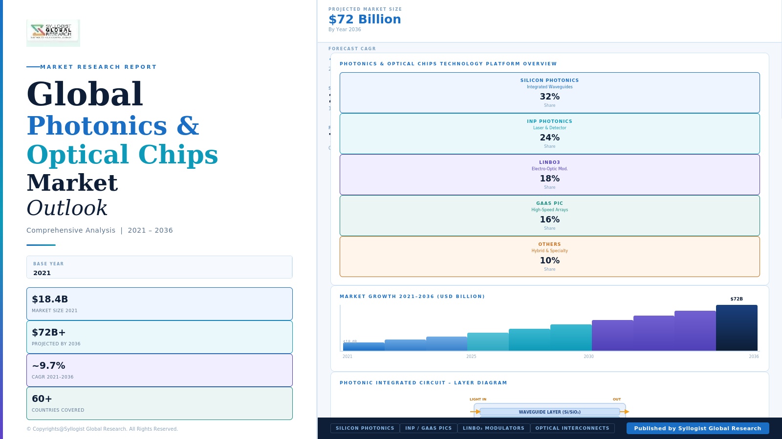
The global photonics and optical chips market was valued at approximately USD 12.4 billion in 2025 and is projected to reach USD 34.7 billion by 2034, advancing at a compound annual growth rate of 12.1% over the forecast period from 2027 to 2034, driven by the convergence of exponentially growing data centre optical interconnect bandwidth demand from artificial intelligence workload expansion, the accelerating commercial deployment of coherent optical transceivers in telecommunications network capacity upgrades, and the emerging commercialisation of photonic computing, quantum photonics, and integrated lidar platforms whose aggregate addressable market is expanding the scope of photonic chip application well beyond the communications-centric demand base that has historically defined the industry. The structural driver underlying these diverse application growth vectors is the fundamental physical advantage of photons over electrons for high-bandwidth, low-latency, and energy-efficient signal transmission and processing over distances from micrometres within co-packaged optics configurations to thousands of kilometres across transoceanic fibre networks, creating a compounding competitive advantage for photonic solutions relative to purely electronic alternatives as data volume, bandwidth density, and energy efficiency requirements continue to escalate across every tier of the global digital infrastructure.
Data centre optical interconnects represent the largest and most commercially dynamic application segment within the global photonics and optical chips market, with hyperscale data centre operators constructing artificial intelligence training clusters of unprecedented scale that require optical connectivity between tens of thousands of graphics processing units and artificial intelligence accelerators at aggregate bisection bandwidths measured in petabits per second, driving optical transceiver procurement at volumes and bandwidth specifications that are defining a new commercial frontier for silicon photonics foundry capacity and co-packaged optics integration technology. The transition from pluggable optical transceiver modules toward co-packaged optics architectures, in which optical components are integrated directly within switch and network interface card packages rather than connected through electrical traces on printed circuit boards, is the most commercially transformative technology development in the data centre photonics segment, with co-packaged optics eliminating the electrical bandwidth bottleneck and power dissipation penalty of the serialiser-deserialiser circuits that govern pluggable transceiver system performance at 800-gigabit and 1.6-terabit port speeds. Coherent optical transceiver chips for long-haul and metro telecommunications networks are growing at approximately 13.4% annually, driven by the capacity upgrade programs of telecommunications carriers and wholesale optical transport network operators whose fibre route utilisation is approaching the spectral efficiency limits of installed erbium-doped fibre amplifier plant, requiring deployment of next-generation coherent transceivers incorporating probabilistic constellation shaping, digital signal processing chips at advanced nodes, and silicon photonic modulator arrays operating at symbol rates above 100 gigabaud that push the boundaries of integrated photonic device performance.
The lidar photonics segment is transitioning from the automotive autonomous driving pilot application that drove the first wave of commercial lidar chip development toward a broader industrial and robotic sensing market whose aggregate demand for solid-state lidar chips is growing at approximately 18.9% annually, encompassing warehouse automation, last-mile delivery robotics, construction site machine guidance, aerial survey systems, smart infrastructure monitoring, and agricultural field mapping applications where the cost reduction and reliability improvement associated with photonic integrated circuit-based lidar relative to mechanical scanning lidar systems are enabling commercial deployments at volume and price points previously unachievable with discrete optic lidar designs. Silicon photonics has emerged as the dominant platform technology for data centre optical transceiver integration, leveraging the manufacturing infrastructure and process maturity of semiconductor silicon wafer fabrication to produce photonic devices at volume and cost scales that compound semiconductor photonic platforms based on indium phosphide or gallium arsenide cannot match, with silicon photonics transceiver chip production at leading foundries approaching volumes of several million units annually and enabling per-chip economics that have reduced 400-gigabit optical transceiver module prices below USD 200 per unit, a price point at which large-scale data centre optical fabric deployment becomes economically accessible to a much broader range of cloud service provider and enterprise data centre operators than was served by the higher-cost discrete component transceiver technology of the prior generation. Indium phosphide photonic integrated circuits retain an irreplaceable competitive position in coherent optical communications applications requiring the highest modulation bandwidth and lowest noise performance that silicon’s indirect bandgap and carrier absorption mechanisms cannot achieve, with indium phosphide photonic integrated circuit wafer processing capacity concentrated in a small number of specialist foundries in North America and Europe that serve the coherent transceiver and microwave photonics segments whose performance requirements exceed the capability boundaries of silicon photonics platforms.
Photonic computing represents the most strategically disruptive emerging application within the global photonics and optical chips market, with photonic tensor processing units that perform matrix multiplication using optical interference in waveguide arrays capable of completing multiply-accumulate operations at the speed of light with energy consumption per operation measured in attojoules compared to femtojoule-scale energy consumption of electronic digital circuits, providing a theoretical efficiency advantage of two to three orders of magnitude for linear algebra operations that constitute the majority of artificial intelligence inference computation and whose energy efficiency is increasingly constraining the economic scalability of conventional electronic artificial intelligence accelerator data centres. Quantum photonic chips are advancing from university research demonstrations toward pre-commercial and early commercial deployments in quantum key distribution networks, quantum computing prototypes, and quantum sensing instruments, with photon-based quantum information processing leveraging room-temperature operation capability, low decoherence rates for photonic qubits, and the compatibility of optical quantum channels with existing fibre telecommunications infrastructure to position photonic approaches competitively relative to superconducting and trapped ion qubit platforms in specific quantum communication and sensing applications. The microwave photonics segment, encompassing photonic analog-to-digital conversion, photonic beamforming for phased array radar and electronic warfare systems, and photonic signal distribution for large-aperture antenna arrays, is generating growing defence procurement investment with the United States Department of Defense and equivalent European and Asian defence programs investing in photonic integrated circuit-based radar and electronic warfare components whose size, weight, power, and electromagnetic interference performance advantages over purely electronic signal processing systems are particularly compelling in airborne and shipborne applications where platform constraints on these parameters are most stringent.
Key Drivers
Artificial Intelligence Data Centre Optical Interconnect Bandwidth Explosion and Co-Packaged Optics Transition Creating Unprecedented Silicon Photonics Demand at Scale
The exponential expansion of artificial intelligence training cluster scale, with hyperscale operators constructing clusters interconnecting 100,000 to 400,000 graphics processing units and artificial intelligence accelerators whose aggregate inter-node optical bandwidth requirements reach several petabits per second within a single facility, is generating optical transceiver procurement volumes and port bandwidth specifications that represent both a massive near-term demand catalyst and a technology forcing function compelling the transition to co-packaged optics architectures whose silicon photonics integration requirement is creating a structural expansion of the photonic chip market well beyond the historical transceiver module replacement cycle that previously defined data centre optical procurement patterns. A single hyperscale artificial intelligence training cluster deploying 100,000 graphics processing units with 800-gigabit optical transceivers on every port represents optical transceiver component procurement of approximately USD 2.4 billion to USD 3.8 billion for the interconnect fabric alone, with the transition to 1.6-terabit and co-packaged optics architectures further increasing photonic chip content per port as optical functions are integrated closer to the silicon die and the number of optical lanes per port increases. The power consumption of electrical serialiser-deserialiser circuits at 800-gigabit and 1.6-terabit port speeds is driving the adoption of co-packaged optics as a power and thermal management imperative as much as a bandwidth enabler, with co-packaged optics eliminating approximately 5 to 8 watts per port of serialiser-deserialiser power dissipation relative to pluggable transceiver alternatives at 800-gigabit port speeds, generating aggregate facility power savings of several megawatts per large-scale artificial intelligence cluster that provide a compelling energy cost and infrastructure capacity justification for co-packaged optics adoption independent of the bandwidth performance improvement it enables.
Telecommunications Network Capacity Upgrade Cycle and Coherent Optical Technology Generation Transition Sustaining Long-Term Photonic Chip Revenue Growth
The ongoing capacity upgrade cycle of global fibre optic telecommunications networks, driven by the 30% to 40% annual growth of internet traffic demand across long-haul, metro, and access network segments, is sustaining a multi-year coherent optical transceiver procurement cycle at telecommunications carriers, internet exchange operators, and submarine cable system owners whose network upgrade programs deploy next-generation photonic integrated circuit-based coherent transceivers operating at progressively higher spectral efficiencies and symbol rates that extract greater capacity from existing fibre plant without the capital cost of installing additional fibre routes. The deployment of 400-gigabit ZR and OpenZR plus coherent transceivers in metro and data centre interconnect applications, and 800-gigabit coherent technology in long-haul backbone and submarine cable applications, is generating photonic integrated circuit procurement demand whose addressable market extends beyond the small number of specialist coherent optical equipment manufacturers that historically represented the sole procurement channel for high-performance indium phosphide and silicon photonics coherent components to include a growing population of data centre operators, network disaggregation platform providers, and web-scale technology companies deploying disaggregated optical networking equipment that incorporates industry-standard coherent optical module specifications. The 5G mobile network densification programs and the emerging 6G technology research investments of major telecommunications equipment manufacturers are generating radio frequency photonic integration demand for remote radio head optical fronthaul, photonic beamforming, and millimetre-wave signal distribution systems whose photonic integrated circuit content per base station is growing with each successive radio access network technology generation and expanding the telecommunications photonic chip market beyond the core transport network transceiver segment that has historically dominated telecommunications photonic procurement.
Lidar Commercialisation Across Automotive, Industrial Robotics, and Infrastructure Sensing Driving Solid-State Photonic Chip Volume Production Ramp
The automotive industry’s commitment to advanced driver assistance system deployment and the gradual commercialisation of higher-level autonomous driving capability is driving a sustained and growing procurement of lidar sensor systems whose evolution from mechanically scanned discrete component designs toward photonic integrated circuit-based solid-state platforms is creating a high-volume commercial market for lidar photonic chips whose manufacturing scale requirements are motivating foundry investment in process capabilities and volume capacity specifically optimised for lidar photonic device production. Automotive lidar system unit shipments reached approximately 4.8 million units in 2025 across driver assistance system and autonomous vehicle prototype applications, with solid-state photonic integrated circuit-based flash lidar and frequency-modulated continuous wave lidar chips growing at approximately 22.3% annually as automotive tier-one suppliers and lidar technology developers commercialise designs that achieve the reliability, operating temperature range, and per-unit cost targets required for passenger vehicle series production integration. The industrial robotics and warehouse automation lidar segment, whose per-application cost sensitivity and operational reliability requirements differ from automotive specifications in ways that have enabled faster solid-state lidar adoption than the more conservative automotive qualification timeline, is growing at approximately 19.1% annually and represents a commercially significant near-term volume production driver for lidar photonic chips that is complementing automotive lidar demand growth and collectively justifying the foundry capacity investment required to achieve the manufacturing scale economies that will enable automotive lidar cost targets of below USD 200 per unit for series production integration by 2028.
Key Challenges
Photonic Chip Packaging Complexity, Optical Fibre Coupling Loss, and Co-Packaged Optics Manufacturing Readiness Constraining Volume Production Ramp
The packaging of photonic integrated circuits presents fundamentally more complex engineering and manufacturing challenges than conventional electronic integrated circuit packaging, with the requirement to couple optical signals between photonic chip waveguides and optical fibres, free-space optical components, or co-integrated laser sources at alignment tolerances measured in sub-micron displacements and angular accuracies below 0.1 degrees whose maintenance over product lifetime in the presence of thermal expansion, mechanical shock, and vibration requires hermetic sealing, precision passive alignment structures, and active alignment verification during assembly that add substantially to packaging cost and complexity relative to purely electronic chip packaging operations whose interconnect tolerances are several orders of magnitude less demanding. Co-packaged optics integration, which requires attaching optical fibre arrays or fibre connectors directly to silicon photonics chips co-packaged with switch or network interface card silicon at sub-micron alignment accuracy within a flip chip assembly process environment that was not designed for optical alignment operations, represents a manufacturing integration challenge that has delayed co-packaged optics volume production ramp significantly beyond the timelines projected by early technology demonstrators, with production-qualified co-packaged optics switch packages achieving commercial availability only in 2024 to 2025 and with manufacturing yield and cost performance still maturing toward the economics required for broad hyperscale data centre deployment. The absence of industry-standardised optical interface specifications for co-packaged optics that would enable multi-vendor silicon photonics die sourcing and optical connector standardisation analogous to the pluggable transceiver multi-source agreements that enabled the pluggable optics ecosystem is creating proprietary coupling architecture fragmentation that constrains supply chain flexibility and increases customer technology lock-in risk.
Compound Semiconductor Substrate Availability, Indium Phosphide Wafer Supply Concentration, and Materials Cost Barriers for Non-Silicon Photonic Platforms
Photonic integrated circuits requiring the highest optical gain, modulation bandwidth, and detection sensitivity performance characteristics that silicon photonics cannot achieve due to silicon’s indirect bandgap must be fabricated on compound semiconductor substrates including indium phosphide, gallium arsenide, and gallium nitride whose wafer supply is served by a small number of specialist compound semiconductor material producers concentrated in Germany, Japan, the United Kingdom, and the United States, creating supply concentration risks and material cost barriers that constrain the commercialisation trajectory of high-performance photonic applications dependent on these material platforms. Indium phosphide wafers, which are required for the fabrication of coherent optical transmitter and receiver photonic integrated circuits whose electro-optic modulation bandwidth and laser integration capability are essential for 400-gigabit and 800-gigabit coherent transceiver applications, are produced at four-inch and six-inch wafer diameters compared to the 300-millimetre wafer standard of leading silicon foundries, with the smaller wafer size imposing a structural die cost disadvantage of three to five times relative to equivalent function silicon photonics dies that constrains the addressable market for indium phosphide photonic integrated circuits to applications whose performance requirements cannot be satisfied by silicon alternatives and where system-level value justifies the higher component cost. The development of heterogeneous integration approaches that bond indium phosphide laser and amplifier chips onto silicon photonic platforms is the primary technology strategy for overcoming the performance limitations of purely silicon-based photonics while retaining the cost and manufacturing scalability advantages of silicon wafer processing, but the wafer bonding process yield, thermal budget compatibility, and reliability qualification requirements of heterogeneous photonic integration add development complexity that extends commercialisation timelines.
Photonic Electronic Design Automation Tool Immaturity, Foundry Process Design Kit Fragmentation, and Photonic-Electronic Co-Design Workflow Complexity Constraining Fabless Chip Development
The photonic integrated circuit design ecosystem lacks the mature electronic design automation tool infrastructure, standardised process design kit library ecosystems, and verified simulation model accuracy that the electronic semiconductor industry has developed over five decades of design tool investment, creating a structural design productivity gap that constrains the pace at which fabless photonic chip design companies can develop, verify, and tape out complex photonic integrated circuits within the development timelines and engineering team scales that venture capital and corporate investment funding assumptions require for commercially viable photonic chip startups and product programs. The absence of a dominant photonic integrated circuit design automation platform analogous to Cadence or Synopsis in electronic design means that photonic chip designers must use fragmented and partially integrated tool flows combining multiple specialised software packages for optical waveguide simulation, active device modelling, circuit-level photonic simulation, and physical layout verification, with limited automated design rule checking, parameter extraction, and back-annotation capability that forces extensive manual verification effort and constrains design team productivity relative to electronic chip design workflows at equivalent circuit complexity levels. The diversity of photonic foundry platforms including silicon photonics, indium phosphide, silicon nitride, and lithium niobate, each with distinct process design kit specifications, waveguide geometry rules, and device performance models that are incompatible across platforms, means that photonic chip designs developed for one foundry process cannot be migrated to alternative foundries without extensive redesign, creating vendor lock-in that limits supply chain flexibility, reduces competitive foundry pricing pressure, and concentrates technology development investment in ways that slow the overall pace of photonic integrated circuit commercialisation across the industry.
Market Segmentation
- Segmentation By Photonic Platform Technology
- Silicon Photonics (SiPh)
- Indium Phosphide (InP) Photonic Integrated Circuits
- Gallium Arsenide (GaAs) Photonic Devices
- Silicon Nitride (Si3N4) Waveguide Platforms
- Lithium Niobate on Insulator (LNOI)
- Gallium Nitride (GaN) Photonics
- Hybrid and Heterogeneous Integration Platforms
- Others
- Segmentation By Device Type
- Optical Transceivers and Transmitters
- Photonic Integrated Circuits (PICs) for Coherent Communications
- Vertical-Cavity Surface-Emitting Lasers (VCSELs)
- Edge-Emitting Lasers and Distributed Feedback Lasers
- Photodetectors and Avalanche Photodiodes
- Optical Modulators (Electro-Optic and Electro-Absorption)
- Optical Switches, Splitters, and Multiplexers
- Lidar Photonic Chips (Frequency-Modulated Continuous Wave and Flash)
- Photonic Computing and Tensor Processing Chips
- Quantum Photonic Chips
- Others
- Segmentation By Application
- Data Centre Optical Interconnects (Pluggable and Co-Packaged)
- Long-Haul and Metro Coherent Optical Communications
- 5G and Wireless Fronthaul and Midhaul
- Lidar for Automotive ADAS and Autonomous Vehicles
- Lidar for Industrial Robotics and Sensing
- Photonic Artificial Intelligence Computing
- Quantum Photonic Computing and QKD
- Biomedical Imaging and Spectroscopy
- Microwave Photonics and Defence Systems
- Consumer and Industrial Sensing
- Others
- Segmentation By Data Rate and Bandwidth
- Below 100 Gbps Optical Devices
- 100 Gbps to 400 Gbps Optical Devices
- 400 Gbps to 800 Gbps Optical Devices
- 800 Gbps to 1.6 Tbps Optical Devices
- Above 1.6 Tbps and Co-Packaged Optics Devices
- Segmentation By Service Model
- Captive Vertically Integrated Manufacturer
- Fabless Photonic Design with Foundry Services
- Photonic Foundry Pure-Play Services
- Photonic Module and Subsystem Integration Services
- Co-Packaged Optics Integration Services
- Segmentation By End-Use Industry
- Hyperscale and Cloud Data Centres
- Telecommunications Carriers and Network Operators
- Automotive and Mobility
- Industrial Automation and Robotics
- Defence, Aerospace, and Government
- Healthcare and Life Sciences
- Consumer Electronics
- Research and Quantum Technology
- Segmentation By Packaging Format
- Pluggable Optical Transceiver Modules (QSFP, OSFP, and CDFP)
- Co-Packaged Optics (CPO) Integrated Packages
- Bare Die and Chip-on-Board Photonics
- Hermetically Sealed Butterfly and Kovar Packages
- Wafer-Level Photonic Packaging
- Segmentation By Region
- Asia-Pacific (China, Taiwan, Japan, South Korea, and Others)
- North America (United States and Canada)
- Europe (Germany, United Kingdom, Netherlands, and Others)
- Rest of World
All market revenues are presented in USD
Historical Year: 2021-2024 | Base Year: 2025 | Estimated Year: 2026 | Forecast Period: 2027-2034
Key Questions this Study Will Answer
- What is the total global market valuation of the Photonics and Optical Chips Market in the base year 2025, and what is the projected market size and compound annual growth rate through 2034, disaggregated by platform technology, silicon photonics, indium phosphide, gallium arsenide, silicon nitride, and lithium niobate, by application, data centre interconnects, coherent telecommunications, lidar, photonic computing, quantum photonics, and defence, and by geography, to enable photonic chip developers, foundry service providers, system integrators, and investors to identify which technology platforms and application segments will generate the highest absolute revenue and most commercially significant adoption momentum across the forecast period?
- How is the transition from pluggable optical transceivers to co-packaged optics architectures expected to reshape the data centre photonics market competitive dynamics, supply chain structure, and silicon photonics foundry capacity investment requirements through 2034, what are the manufacturing readiness and yield performance benchmarks that co-packaged optics production programs must achieve to enable broad hyperscale deployment, which silicon photonics platform and optical interface standardisation developments are most critical to enabling a multi-vendor co-packaged optics supply ecosystem, and how are leading hyperscale operators, switch silicon developers, and optical module manufacturers positioning their co-packaged optics technology partnerships and supply chain strategies?
- What is the projected commercial trajectory of solid-state lidar photonic chips across automotive driver assistance, autonomous vehicle, industrial robotics, and infrastructure sensing applications through 2034, at what per-unit cost and performance benchmarks will frequency-modulated continuous wave and flash lidar photonic integrated circuits achieve the automotive series production integration economics required for broad passenger vehicle deployment, which photonic platform technologies and foundry manufacturing approaches are best positioned to deliver the cost reduction roadmap required for mass-market lidar, and how will the aggregate lidar photonic chip market evolve as automotive and industrial demand segments develop at different adoption pace and volume trajectories?
- How are photonic computing accelerators and quantum photonic chips expected to transition from research and early commercial demonstration toward volume production through 2034, what are the optical loss, modulation efficiency, and photon number resolution performance thresholds that photonic computing and quantum photonic chips must achieve to deliver commercially competitive performance relative to electronic and other qubit technology alternatives, which application domains are generating the most credible near-term commercial deployment opportunities for photonic computing and quantum photonics, and what are the foundry capability and packaging technology development requirements for supporting volume production of these emerging photonic chip categories?
- Who are the leading silicon photonics platform developers, indium phosphide and compound semiconductor photonic chip manufacturers, photonic foundry service providers, lidar chip developers, coherent transceiver photonic integrated circuit companies, and photonic computing technology pioneers currently defining the competitive landscape of the global photonics and optical chips market, and what are their respective technology platform coverage and process node capabilities, customer program engagement with hyperscale data centre operators and telecommunications equipment manufacturers, research and development investment in co-packaged optics and next-generation coherent modulation technology, foundry capacity expansion programs, and competitive positioning responses to the packaging complexity, compound semiconductor supply, and design tool maturity challenges shaping photonic chip market development through 2034?
- Product Definition
- Research Methodology
- Research Design & Framework
- Overall Research Approach: Descriptive, Exploratory & Quantitative Mixed-Method Design
- Market Definition & Scope Boundaries: What is Included and Excluded
- Segmentation Framework
- Key Research Assumptions & Limitations
- Secondary Research
- Primary Research Design & Execution
- Data Triangulation & Validation
- Market Sizing & Forecasting Methodology
- Competitive Intelligence Methodology
- Quality Assurance & Peer Review
- Definitions, Abbreviations & Data Notes
- Research Design & Framework
- Executive Summary
- Market Snapshot & Headline Numbers
- Key Findings & Research Highlights
- Market Dynamics
- Regional Market Summary
- Competitive Landscape Snapshot
- Technology & Innovation Highlights
- Market Dynamics
- Drivers
- Restraints
- Opportunities
- Challenges
- Porter’s Five Forces Analysis
- PESTLE Analysis
- Market Trends & Developments
- Emerging Trends
- Technological Developments
- Regulatory & Policy Changes
- Supply Chain & Sourcing Trends
- Manufacturing & Process Trends
- Investment & Funding Activity
- Sustainability & ESG Trends
- Risk Assessment Framework
- Geopolitical, Export Control & Critical Material Supply Concentration Risk
- Technology Substitution, Competing Interconnect Architecture & Ecosystem Fragmentation Risk
- Manufacturing Yield, Wafer Fabrication Process Maturity & Scale-Up Risk
- Capital Intensity, R&D Investment Cycle & Commercialisation Timeline Risk
- Standardisation, Interoperability & Multi-Vendor Ecosystem Integration Risk
- Regulatory Framework & Standards
- Export Controls & Dual-Use Technology Restrictions on Photonic Integrated Circuits & Optical Components
- IEEE, IEC, ITU & Industry Standards for Optical Interconnects, Silicon Photonics & Photonic Integrated Circuits
- Eye Safety, Laser Classification & IEC 60825 Regulatory Requirements for Optical Chip Products
- Government R&D Funding Programmes, National Photonics Strategies & Domestic Manufacturing Incentives
- Environmental Regulations: RoHS, REACH & Hazardous Substance Standards in Photonic Component Manufacturing
- Global Photonics & Optical Chips Market Outlook
- Market Size & Forecast by Value
- Market Size & Forecast by Volume (Units)
- Market Size & Forecast by Product Type
- Silicon Photonics Integrated Circuits (SiPh ICs)
- Indium Phosphide (InP) Photonic Integrated Circuits
- Gallium Arsenide (GaAs) Photonic Integrated Circuits
- Lithium Niobate on Insulator (LNOI) Photonic Chips
- Optical Transceivers & Co-Packaged Optics (CPO) Modules
- Laser-on-Silicon & Hybrid Laser Chips
- Optical Modulators & Electro-Optic Chips
- Photodetectors & Optical Receiver Chips
- Photonic MEMS & Tunable Optical Chips
- Quantum Photonic Chips
- Market Size & Forecast by Material Platform
- Silicon-on-Insulator (SOI)
- Indium Phosphide (InP)
- Gallium Arsenide (GaAs) & Gallium Nitride (GaN)
- Lithium Niobate (LN)
- Silicon Nitride (SiN)
- Polymer & Organic Photonic Platforms
- Hybrid & Heterogeneous Integration Platforms
- Market Size & Forecast by Technology
- Photonic Integrated Circuit (PIC) Fabrication Technology
- Co-Packaged Optics (CPO) & Near-Package Optics Integration Technology
- Wafer Bonding & Heterogeneous Integration Technology
- Optical Beamforming & Phased Array Technology
- Wavelength Division Multiplexing (WDM) & Dense WDM Technology
- Nonlinear Photonics, Frequency Comb & Optical Signal Processing Technology
- Quantum Photonics & Entangled Photon Source Technology
- Market Size & Forecast by Integration Level
- Discrete Optical Components
- Small-Scale Photonic Integrated Circuits (Below 10 Functional Elements)
- Medium-Scale Photonic Integrated Circuits (10 to 100 Functional Elements)
- Large-Scale Photonic Integrated Circuits (Above 100 Functional Elements)
- Market Size & Forecast by End-Use Industry
- Data Centre & Cloud Computing (AI/HPC Optical Interconnects)
- Telecommunications & 5G/6G Network Infrastructure
- Consumer Electronics & Mobile Devices
- Automotive (LiDAR, In-Vehicle Optical Sensing & Connectivity)
- Healthcare & Life Sciences (Optical Coherence Tomography, Biosensing & Medical Imaging)
- Aerospace & Defence (Optical Gyroscopes, LiDAR & Free-Space Communication)
- Industrial Sensing, Metrology & Manufacturing
- Quantum Computing & Quantum Communication
- Market Size & Forecast by Application
- High-Speed Optical Interconnects & Data Transmission
- LiDAR & 3D Sensing
- Optical Coherence Tomography (OCT) & Biomedical Imaging
- Optical Fibre Sensing & Distributed Measurement
- Optical Signal Processing & Neuromorphic Photonics
- Free-Space Optical Communication & Satellite Optical Links
- Quantum Key Distribution (QKD) & Quantum Sensing
- Market Size & Forecast by Sales Channel
- Direct OEM & Hyperscaler Supply Agreements
- Distribution & Value-Added Reseller (VAR) Channel
- Foundry & Pure-Play PIC Fabrication Service Channel
- Systems Integrator & Optical Module Assembly Channel
- North America Photonics & Optical Chips Market Outlook
- Market Size & Forecast
- By Value
- By Volume (Units)
- By Product Type
- By Material Platform
- By Technology
- By End-Use Industry
- By Application
- By Sales Channel
- By Country
- Market Size & Forecast
- Europe Photonics & Optical Chips Market Outlook
- Market Size & Forecast
- By Value
- By Volume (Units)
- By Product Type
- By Material Platform
- By Technology
- By End-Use Industry
- By Application
- By Sales Channel
- By Country
- Market Size & Forecast
- Asia-Pacific Photonics & Optical Chips Market Outlook
- Market Size & Forecast
- By Value
- By Volume (Units)
- By Product Type
- By Material Platform
- By Technology
- By End-Use Industry
- By Application
- By Sales Channel
- By Country
- Market Size & Forecast
- Latin America Photonics & Optical Chips Market Outlook
- Market Size & Forecast
- By Value
- By Volume (Units)
- By Product Type
- By Material Platform
- By Technology
- By End-Use Industry
- By Application
- By Sales Channel
- By Country
- Market Size & Forecast
- Middle East & Africa Photonics & Optical Chips Market Outlook
- Market Size & Forecast
- By Value
- By Volume (Units)
- By Product Type
- By Material Platform
- By Technology
- By End-Use Industry
- By Application
- By Sales Channel
- By Country
- Market Size & Forecast
- Country-Wise* Photonics & Optical Chips Market Outlook
- Market Size & Forecast
- By Value
- By Volume (Units)
- By Product Type
- By Material Platform
- By Technology
- By End-Use Industry
- By Application
- By Sales Channel
- By Country
- Market Size & Forecast
- *Countries Analyzed in the Syllogist Global Research Portfolio: United States, Canada, Mexico, Germany, France, United Kingdom, Netherlands, Spain, Italy, Norway, Sweden, China, Japan, India, Australia, South Korea, Singapore, Brazil, Chile, Saudi Arabia, UAE, Egypt, South Africa, Israel
- Technology Landscape & Innovation Analysis
- Silicon Photonics Platform Technology Deep-Dive: SOI Waveguides, Germanium Detectors, Ring Resonators & Monolithic Integration
- Indium Phosphide (InP) PIC Technology: Laser Integration, High-Speed Modulation & Compound Semiconductor Fabrication
- Lithium Niobate on Insulator (LNOI) Technology: Ultra-Low-Loss Waveguides, High-Bandwidth Modulation & Frequency Conversion
- Co-Packaged Optics (CPO) & Near-Package Optics Technology: Architecture, Thermal Management & Ecosystem Development
- Optical Beamforming, Phased Array & Solid-State LiDAR Chip Technology
- Quantum Photonic Chip Technology: Single-Photon Sources, Entanglement Generation & Photonic Qubit Circuits
- Neuromorphic Photonics, All-Optical AI Accelerator & Photonic Computing Architecture Technology
- Patent & IP Landscape in Photonics & Optical Chip Technologies
- Value Chain & Supply Chain Analysis
- Photonic Wafer, Epitaxial Wafer & Substrate Material Supply Chain
- PIC Foundry, Wafer Fabrication & Process Design Kit (PDK) Ecosystem
- Optical Packaging, Fibre Coupling, Lens Array & Assembly Supply Chain
- Test, Characterisation & Reliability Qualification Equipment & Service Supply Chain
- Electronic-Photonic Integration, ASIC Co-Design & EDA Tool Provider Channel
- Optical Module Assembler, Transceiver Manufacturer & System Integration Channel
- End-User OEM, Hyperscaler, Telecom Operator & Defence Procurement Channel
- Pricing Analysis
- Silicon Photonics Chip Wafer Cost, Die Cost & Price-Per-Gbps Analysis
- InP & GaAs PIC Fabrication Cost, Epitaxial Growth Cost & Price Comparison vs. SOI
- Optical Transceiver & Co-Packaged Optics Module Pricing Trend Analysis by Data Rate (100G to 1.6T)
- LiDAR Photonic Chip & Solid-State LiDAR Module Pricing & Cost Reduction Roadmap Analysis
- Optical Packaging, Fibre Attach & Assembly Cost Analysis for PICs
- Total Cost of Ownership & Price-Per-Bit Analysis: Optical Interconnect vs. Copper Electrical Interconnect
- Sustainability & Environmental Analysis
- Lifecycle Assessment (LCA) of Photonic & Optical Chips: Carbon Footprint, Energy Use, Rare Material Consumption & Packaging Waste
- Energy Efficiency of Optical Interconnects vs. Electrical Interconnects: Data Centre Power Reduction & Carbon Impact
- Compound Semiconductor Materials (InP, GaAs): Supply Chain Sustainability, Conflict Mineral Risk & Responsible Sourcing
- Photonics-Enabled Efficiency Gains in Telecommunications, Sensing & Healthcare: Broader Environmental & Social Impact
- Regulatory-Driven Sustainability, Net Zero Manufacturing Commitments & ESG Reporting in the Photonics Industry
- Competitive Landscape
- Market Structure & Concentration
- Market Consolidation Level (Fragmented vs. Consolidated by Product Type, Material Platform & Geography)
- Top 10 Players Market Share
- HHI (Herfindahl-Hirschman Index) Concentration Analysis
- Competitive Intensity Map by Product Type, Technology & Geography
- Player Classification
- Integrated Photonics & Semiconductor Companies with Full PIC Portfolios
- Pure-Play Silicon Photonics Chip Design & Fabless Companies
- InP & Compound Semiconductor PIC Manufacturers
- Optical Transceiver & Co-Packaged Optics Module Companies
- PIC Foundries & Photonic Manufacturing Service Providers
- Quantum Photonics & Emerging Platform Start-ups
- LiDAR & Automotive Optical Chip Specialists
- Competitive Analysis Frameworks
- Market Share Analysis by Product Type, Material Platform & Region
- Company Profile
- Company Overview & Headquarters
- Photonics & Optical Chip Products & Technology Portfolio
- Key Customer Relationships & Reference Design Wins
- Wafer Fabrication Footprint, Foundry Partnerships & Production Capacity
- Revenue (Photonics & Optical Chip Segment) & Backlog
- Technology Differentiators & IP
- Key Strategic Partnerships, JVs & M&A Activity
- Recent Developments (Product Launches, Capacity Expansion, Funding Rounds)
- SWOT Analysis
- Strategic Focus Areas & Roadmap
- Competitive Positioning Map (Technology Capability vs. Market Penetration)
- Key Company Profiles
- Market Structure & Concentration
- Technology Landscape & Innovation Analysis
- Strategic Output
- Market Opportunity Matrix: By Product Type, Material Platform, Technology, End-Use Industry & Geography
- White Space Opportunity Analysis
- Strategic Recommendations
- Product Portfolio & Technology Investment Strategy
- Manufacturing & Operational Excellence Strategy
- Geographic Expansion & Localisation Strategy
- Customer & End-User Engagement Strategy
- Partnership, M&A & Ecosystem Strategy
- Sustainability & Circular Economy Strategy
- Risk Mitigation & Future Roadmap
- Strategic Priority Matrix & Roadmap
- Near-term (2025-2028)
- Mid-term (2029-2032)
- Long-term (2033-2037)
- Strategic Output