Global Probe Cards Market By Product Type, By Technology, By Wafer Size, By Application, By End User, By Region, Competition, Forecast & Opportunities, 2021-2036F
Market Definition
The Global Probe Cards Market covers the design, manufacture, qualification, supply, and aftermarket service of precision interface tooling used during the wafer probe test stage of semiconductor manufacturing to establish temporary electrical connections between automated test equipment and individual integrated circuit die on a semiconductor wafer. Probe cards are consumable interface assemblies built from MEMS-fabricated probes, vertical buckling beam structures, cantilever needle arrays, or advanced spring-loaded contactor technologies mounted on multilayer printed circuit boards, ceramic substrates, or organic interposers, engineered to deliver thousands of simultaneous low-resistance contacts at micron-scale pitch across logic, memory, mixed-signal, RF, power, and image sensor devices. The market encompasses advanced MEMS probe cards used for leading-edge logic and high-bandwidth memory wafer test, vertical probe cards for DRAM and NAND memory production, cantilever probe cards for analog, power semiconductor, and trailing-edge applications, alongside specialized probe cards for RF, optoelectronic, MEMS sensor, and millimeter-wave device test. Probe cards are procured by integrated device manufacturers including Samsung, SK hynix, Micron, Intel, Texas Instruments, Infineon, STMicroelectronics, NXP, Renesas, alongside pure-play foundries TSMC, GlobalFoundries, UMC, SMIC, Tower Semiconductor, and outsourced semiconductor assembly and test providers across the global manufacturing ecosystem. The supplier landscape is concentrated among specialized probe card vendors including FormFactor, Technoprobe, Micronics Japan (MJC), Japan Electronic Materials (JEM), Korea Instrument, MPI Corporation, Feinmetall, SV Probe, Will Technology, TSE Co., TIPS Messtechnik, and emerging Chinese suppliers, with competition shaped by pin count, pitch capability, signal integrity, contact resistance stability, planarity tolerance, and lifetime touchdown count specifications across increasingly demanding wafer test requirements.
Market Insights
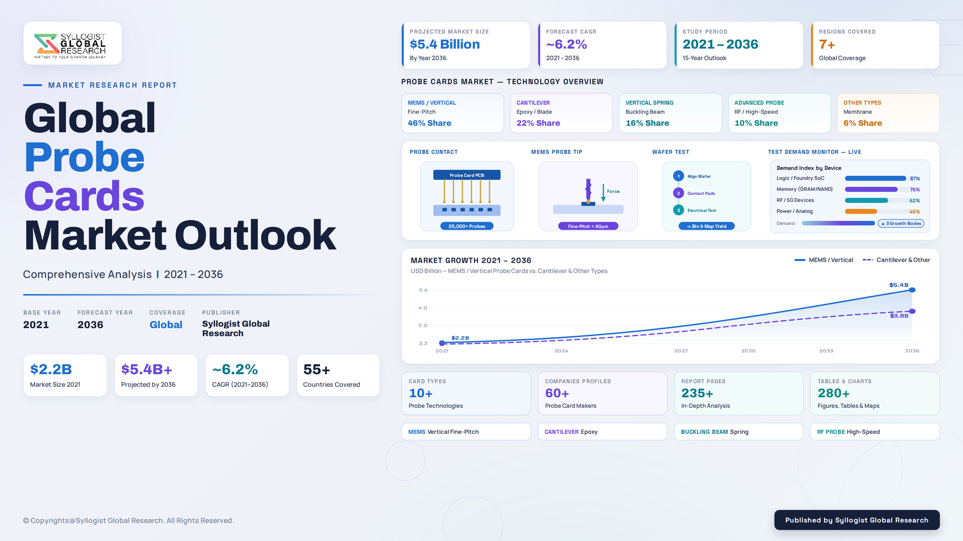
The global probe cards market is entering a sustained high-growth phase, propelled by accelerating leading-edge logic node transitions to 3 nm and 2 nm geometries, the explosive ramp of high-bandwidth memory production supporting AI accelerator demand, the proliferation of advanced packaging architectures including 2.5D and 3D heterogeneous integration, and the structural ramp of automotive semiconductor and silicon carbide power device wafer probe requirements. The market was valued at USD 2.84 billion in 2025 and is projected to reach USD 6.92 billion by 2034, advancing at a compound annual growth rate of 10.4% through the forecast period, supported by rising pin count requirements, shrinking probe pitch specifications, and the structural increase in wafer test complexity at every successive technology node across logic, memory, and specialty device categories.
MEMS probe cards represent the fastest growing product category, advancing at over 12.6% CAGR through 2034, as leading-edge logic at 3 nm and 2 nm, gate-all-around transistor architectures, and increasingly dense bump arrays on advanced packaging substrates require pitch capability below 80 microns and pin counts exceeding 100,000 contacts per probe card. Vertical probe cards remain the dominant category for DRAM, NAND, and high-bandwidth memory wafer test, where pin counts above 60,000 and high-temperature operating capability are essential, with HBM3E and forthcoming HBM4 ramp at SK hynix, Samsung, and Micron driving substantial incremental procurement intensity. Cantilever probe cards continue to anchor analog, power semiconductor, automotive trailing-edge, and image sensor applications, with renewed demand growth driven by silicon carbide and gallium nitride power device production at Infineon, Wolfspeed, onsemi, STMicroelectronics, ROHM, and Mitsubishi Electric across the EV powertrain and industrial electrification value chains.
FormFactor and Technoprobe collectively account for nearly 64% of global probe card revenue in 2025, with FormFactor leading in DRAM and high-bandwidth memory probe card supply, and Technoprobe holding the dominant position in leading-edge MEMS probe cards for advanced logic at TSMC, Samsung Foundry, and Intel Foundry. Japan Electronic Materials, Micronics Japan, MPI Corporation, Feinmetall, SV Probe, and Korea Instrument together represent the next supplier layer with strong positioning across memory, analog, and specialty applications, while emerging Chinese probe card suppliers are advancing rapidly under domestic semiconductor self-sufficiency programs and capturing share across trailing-edge and mature node applications. The cost intensity of probe cards is rising materially with each technology node, with advanced MEMS probe cards for 2 nm logic now exceeding 220,000 USD per unit and HBM4 vertical probe cards approaching 180,000 USD per unit, reshaping consumable cost economics across leading-edge fab and OSAT facilities.
Asia-Pacific dominates the global probe cards market with approximately 74% revenue share in 2025, anchored by Taiwan, South Korea, China, and Japan as the principal demand centers, with Taiwan alone accounting for nearly 28% of global procurement supported by TSMC wafer test capacity expansion across Hsinchu, Tainan, Kaohsiung, Arizona, Kumamoto, and Dresden fab sites. South Korea represents the second largest regional market driven by Samsung and SK hynix DRAM, NAND, and HBM wafer test operations, while China is the fastest growing regional market advancing at over 15.2% CAGR through 2034, supported by SMIC, Hua Hong, YMTC, CXMT, and emerging domestic logic and memory fabs scaling capacity under semiconductor self-sufficiency mandates. North America is rebuilding its share through CHIPS Act incentivized fab projects at Intel Ohio, TSMC Arizona, Samsung Taylor, Micron Boise and Syracuse, while Europe is advancing capacity additions at TSMC Dresden, Intel Magdeburg, Infineon Villach, and STMicroelectronics Catania.
Key Drivers
Leading-Edge Logic Node Transitions to 3 nm, 2 nm, and Sub-2 nm Architectures Multiplying Probe Card Pin Count and Pitch Requirements
Each successive logic node transition is materially increasing probe card pin count, pitch density, and signal integrity requirements, with leading-edge MEMS probe cards for 2 nm and Angstrom-class production at TSMC, Samsung Foundry, and Intel Foundry now requiring pin counts above 100,000 contacts and pitch below 80 microns. Capital programs anchored at TSMC Hsinchu, Samsung Pyeongtaek, and Intel Ohio fabs are driving sustained MEMS probe card procurement, with advanced node probe card spend rising materially per wafer tested through the forecast horizon to 2034.
High-Bandwidth Memory, AI Accelerator, and DRAM Density Growth Driving Vertical Probe Card Procurement Intensity
Explosive HBM3E and forthcoming HBM4 ramp at SK hynix, Samsung, and Micron in support of NVIDIA, AMD, Intel, Broadcom, and hyperscaler custom silicon AI accelerator programs is driving sustained vertical probe card procurement intensity across memory wafer test. DRAM density transitions to 1b nm and 1c nm and 3D NAND scaling beyond 300 layers are increasing pin count above 60,000 contacts, with HBM-dedicated probe card procurement projected to advance at 13.8% CAGR through 2034 across Pyeongtaek, Icheon, Cheongju, Boise, and Hiroshima memory fabs.
Silicon Carbide, Gallium Nitride, and Automotive Power Semiconductor Wafer Test Driving Cantilever Probe Card Demand Resurgence
Silicon carbide and gallium nitride power device production ramping at Infineon, Wolfspeed, onsemi, STMicroelectronics, ROHM, and Mitsubishi Electric in support of EV powertrain, industrial electrification, and renewable energy inverter demand is driving a resurgence in cantilever probe card procurement. Automotive semiconductor wafer test demand at NXP, Renesas, Texas Instruments, and Microchip is simultaneously scaling, with combined power and automotive cantilever probe card spend projected to advance at 9.6% CAGR through 2034 as SiC 200 mm wafer adoption and GaN power module production scale.
Key Challenges
US Export Controls on Advanced Semiconductor Test Equipment Shipments to China Constraining Supplier Revenue and Reshaping Trade Architecture
US Department of Commerce export controls covering advanced semiconductor manufacturing and test equipment shipments to China, expanded across 2022, 2023, and 2024 to include sub-14 nm logic and advanced memory production tooling, are constraining probe card supplier revenue exposure to Chinese leading-edge fabs and reshaping trade architecture. FormFactor, Technoprobe, and Japanese probe card suppliers have each disclosed China revenue impacts ranging from 12% to 28%, while emerging Chinese probe card suppliers are accelerating share capture across trailing-edge categories as Chinese fabs aggressively qualify domestic alternatives.
Probe Card Cost Intensity Escalation, Yield Loss Sensitivity, and Touchdown Lifetime Constraints Pressuring Fab Consumable Economics
Probe card cost per unit is rising materially with each technology node, with advanced MEMS probe cards for 2 nm logic now exceeding 220,000 USD per unit and HBM4 vertical probe cards approaching 180,000 USD per unit, reshaping fab and OSAT consumable cost economics. Touchdown lifetime constraints, planarity degradation under repeated contact cycles, and the rising frequency of probe card refurbishment intervals are introducing operational complexity that complicates wafer test cost modeling, yield management, and capacity planning at leading-edge fabs and major OSAT operators.
Skilled Engineering Talent Shortages, Lead Time Extensions, and Aftermarket Service Capacity Constraints Limiting Supplier Responsiveness
Structural shortages of probe card design engineers, MEMS process specialists, and qualified field service technicians across Taiwan, South Korea, Japan, and emerging fab locations are extending probe card design-to-delivery lead times from 6 to 8 weeks historically toward 12 to 16 weeks for advanced MEMS configurations. Aftermarket service capacity, probe tip refurbishment turnaround, and engineering response times remain critical bottlenecks, with TSMC Arizona, Intel Ohio, and Samsung Taylor reporting wafer test ramp timeline extensions partially attributable to probe card supply constraints.
Market Segmentation
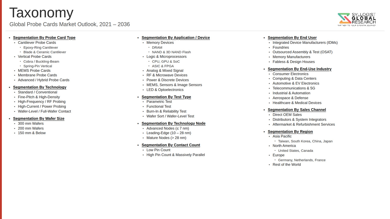
- Segmentation By Product Type
- MEMS Probe Cards
- Vertical Probe Cards
- Cantilever Probe Cards
- Spring-Loaded Contactor Probe Cards
- Hybrid and Specialty Probe Cards
- Others
- Segmentation By Technology
- Advanced MEMS (Sub-80 Micron Pitch)
- Vertical Buckling Beam
- Cantilever Needle Arrays
- Pogo Pin and Spring Contactor
- RF and Millimeter-Wave Probe Cards
- Optical and Photonic Probe Cards
- Others
- Segmentation By Wafer Size
- 150 mm and Below
- 200 mm
- 300 mm
- Emerging 450 mm and Panel Substrates
- Others
- Segmentation By Application
- Logic and SoC Wafer Test
- DRAM Wafer Test
- NAND Flash Wafer Test
- High-Bandwidth Memory (HBM) Wafer Test
- Analog and Mixed-Signal Test
- RF and Millimeter-Wave Device Test
- Power Semiconductor (SiC, GaN, Silicon) Test
- MEMS, Sensor, and Image Sensor Test
- Optoelectronic and Photonic Device Test
- Others
- Segmentation By End User
- Integrated Device Manufacturers (IDMs)
- Foundries
- Memory Manufacturers
- Outsourced Semiconductor Assembly and Test (OSAT)
- Fabless and Test Houses
- Research Institutions
- Others
- Segmentation By Region
- Asia-Pacific (Taiwan, South Korea, China, Japan, Southeast Asia)
- North America
- Europe
- Middle East and Africa
- Latin America
All market revenues are presented in USD
Historical Year: 2021-2024 | Base Year: 2025 | Estimated Year: 2026 | Forecast Period: 2027-2034
Key Questions this Study Will Answer
- What is the total market valuation of the Global Probe Cards Market in 2025, projected through 2034, disaggregated by product type, technology, application, and end user, enabling probe card suppliers, fab operators, OSAT providers, and investors to identify the highest-growth opportunities and most durable revenue corridors across the probe card value chain?
- How are leading-edge logic node transitions to 3 nm, 2 nm, and sub-2 nm geometries, gate-all-around transistor architectures, and EUV adoption multiplying probe card pin count, pitch capability, and signal integrity requirements across TSMC, Samsung Foundry, and Intel Foundry advanced wafer test operations through 2034?
- Which probe card categories including MEMS probe cards, vertical probe cards, cantilever probe cards, spring-loaded contactor probe cards, and specialty RF and millimeter-wave probe cards are generating the highest growth rates, and how are technology transitions reshaping competitive positioning across FormFactor, Technoprobe, Japan Electronic Materials, Micronics Japan, MPI Corporation, Feinmetall, SV Probe, and Korea Instrument?
- How is high-bandwidth memory ramp including HBM3E and forthcoming HBM4 at SK hynix, Samsung, and Micron, alongside AI accelerator demand at NVIDIA, AMD, Intel, Broadcom, Google, Microsoft, Amazon, and Meta, driving vertical probe card procurement intensity across Pyeongtaek, Icheon, Cheongju, Boise, and Hiroshima memory fabs?
- How are silicon carbide and gallium nitride power device production ramping at Infineon, Wolfspeed, onsemi, STMicroelectronics, ROHM, and Mitsubishi Electric, alongside automotive semiconductor wafer test scaling at NXP, Renesas, Texas Instruments, and Microchip, driving cantilever probe card demand resurgence through 2034?
- How are US export controls on advanced semiconductor manufacturing and test equipment shipments to China reshaping probe card supplier revenue exposure, market share dynamics, and competitive positioning across leading-edge and trailing-edge categories, and how are emerging Chinese probe card suppliers capturing share through 2034?
- How are CHIPS Act, European Chips Act, and Asia-Pacific semiconductor self-sufficiency programs driving probe card procurement across Arizona, Ohio, Taylor, Boise, Magdeburg, Dresden, Kumamoto, Hsinchu, Pyeongtaek, and Chinese fab projects, and what regional demand patterns are emerging through 2034?
- Product Definition
- Research Methodology
- Research Design & Framework
- Overall Research Approach: Descriptive, Exploratory & Quantitative Mixed-Method Design
- Market Definition & Scope Boundaries: What is Included and Excluded
- Segmentation Framework
- Key Research Assumptions & Limitations
- Secondary Research
- Primary Research Design & Execution
- Data Triangulation & Validation
- Market Sizing & Forecasting Methodology
- Competitive Intelligence Methodology
- Quality Assurance & Peer Review
- Definitions, Abbreviations & Data Notes
- Research Design & Framework
- Executive Summary
- Market Snapshot & Headline Numbers
- Key Findings & Research Highlights
- Market Dynamics
- Regional Market Summary
- Competitive Landscape Snapshot
- Technology & Innovation Highlights
- Market Dynamics
- Drivers
- Restraints
- Opportunities
- Challenges
- Porter’s Five Forces Analysis
- PESTLE Analysis
- Market Trends & Developments
- Emerging Trends
- Technological Developments
- Regulatory & Policy Changes
- Supply Chain & Sourcing Trends
- Manufacturing & Process Trends
- Investment & Funding Activity
- Sustainability & ESG Trends
- Risk Assessment Framework
- Semiconductor Cyclicality, Capex Volatility & Demand Concentration Risk
- Raw Material, Precision Component & Specialty Material Supply Risk
- Technology Obsolescence, Node Migration & Design Complexity Risk
- Customer Concentration, Qualification Lead-Time & Long Design-In Cycle Risk
- Geopolitical, Export Control & Supply Chain Localisation Risk
- Regulatory Framework & Standards
- Semiconductor Test Interface & Probe Card Industry Standards (SEMI & JEDEC Frameworks)
- Quality, Reliability & Qualification Standards for Wafer-Level Test (ISO, IATF & AEC-Q)
- Material Compliance, RoHS, REACH & Conflict-Minerals Regulations
- Export Control, Trade & Technology Transfer Regulations for Semiconductor Equipment
- Environmental, Worker Safety & Cleanroom Compliance Standards
- Global Probe Cards Market Outlook
- Market Size & Forecast by Value
- Market Size & Forecast by Volume (Units & Shipments)
- Market Size & Forecast by Probe Card Type
- Cantilever Probe Cards
- Vertical Probe Cards
- Vertical MEMS Probe Cards
- Membrane Probe Cards
- Blade Probe Cards
- Epoxy Ring Probe Cards
- Coaxial & RF Probe Cards
- Advanced Spring Contact (Pogo Pin) Probe Cards
- Other & Hybrid Probe Card Types
- Market Size & Forecast by Technology
- MEMS (Micro-Electro-Mechanical Systems) Technology
- Spring Pin & Pogo Pin Technology
- Wire & Needle-Based Contact Technology
- Thin-Film & Membrane Technology
- Vertical Buckling Beam Technology
- Cantilever Needle Technology
- Advanced Probe Tip Materials & Coatings
- Space Transformer & Multilayer Ceramic / Organic Substrate Technology
- Other Emerging & Hybrid Probe Technologies
- Market Size & Forecast by Test Type
- Parametric & DC Test
- Functional & Logic Test
- RF & High-Frequency Test
- Burn-In & Reliability Test
- Wafer-Level & Known Good Die (KGD) Test
- Market Size & Forecast by Parallelism Level
- High Parallelism (Full-Wafer & Many-DUT) Probe Cards
- Medium Parallelism (Multi-DUT) Probe Cards
- Low Parallelism (Single & Few-DUT) Probe Cards
- Market Size & Forecast by Application
- Logic & System-on-Chip (SoC) Testing
- Memory Device (DRAM, NAND & Flash) Testing
- RF, Analog & Mixed-Signal Device Testing
- MEMS & Sensor Testing
- Power Device & Discrete Semiconductor Testing
- CMOS Image Sensor (CIS), LED & Optoelectronics Testing
- Market Size & Forecast by End-User
- Integrated Device Manufacturers (IDMs)
- Pure-Play Foundries
- Outsourced Semiconductor Assembly & Test (OSAT) Providers
- Fabless Companies & Test Houses
- Research Institutes & Other End-Users
- Market Size & Forecast by Sales Channel
- Direct Sales & OEM Supply
- Distributors & Authorised Resellers
- Aftermarket, Refurbishment & Cleaning Services
- Online & Procurement Platforms
- North America Probe Cards Market Outlook
- Market Size & Forecast
- By Value
- By Volume (Units & Shipments)
- By Probe Card Type
- By Technology
- By Test Type
- By Parallelism Level
- By Application
- By End-User
- By Country
- By Sales Channel
- Europe Probe Cards Market Outlook
- Market Size & Forecast
- By Value
- By Volume (Units & Shipments)
- By Probe Card Type
- By Technology
- By Test Type
- By Parallelism Level
- By Application
- By End-User
- By Country
- By Sales Channel
- Asia-Pacific Probe Cards Market Outlook
- Market Size & Forecast
- By Value
- By Volume (Units & Shipments)
- By Probe Card Type
- By Technology
- By Test Type
- By Parallelism Level
- By Application
- By End-User
- By Country
- By Sales Channel
- Latin America Probe Cards Market Outlook
- Market Size & Forecast
- By Value
- By Volume (Units & Shipments)
- By Probe Card Type
- By Technology
- By Test Type
- By Parallelism Level
- By Application
- By End-User
- By Country
- By Sales Channel
- Middle East & Africa Probe Cards Market Outlook
- Market Size & Forecast
- By Value
- By Volume (Units & Shipments)
- By Probe Card Type
- By Technology
- By Test Type
- By Parallelism Level
- By Application
- By End-User
- By Country
- By Sales Channel
- Country-Wise* Probe Cards Market Outlook
- Market Size & Forecast
- By Value
- By Volume (Units & Shipments)
- By Probe Card Type
- By Technology
- By Test Type
- By Parallelism Level
- By Application
- By End-User
- By Country
- By Sales Channel
- *Countries Analyzed in the Syllogist Global Research Portfolio: United States, Canada, Mexico, Germany, France, United Kingdom, Netherlands, Spain, Italy, Norway, Sweden, China, Japan, India, Australia, South Korea, Singapore, Brazil, Chile, Saudi Arabia, UAE, Egypt, South Africa, Israel
- Technology Landscape & Innovation Analysis
- MEMS Probe Card Technology Deep-Dive
- Vertical & Buckling Beam Probe Technology
- Cantilever & Needle-Based Probe Technology
- Advanced Probe Tip Materials, Coatings & Wear Resistance
- Space Transformer, Multilayer Ceramic & Organic Interposer Technology
- Fine-Pitch, High-Parallelism & Full-Wafer Contact Technology
- RF, High-Speed & High-Power Probe Interface Technology
- Patent & IP Landscape in Probe Card Technologies
- Value Chain & Supply Chain Analysis
- Probe Material, Needle & Contact Element Manufacturing Supply Chain
- MEMS Fabrication, Space Transformer & PCB Supply Chain
- Precision Machining, Assembly & Component Supply Chain
- Probe Card Design, Engineering & Customisation Landscape
- ATE Tester, Wafer Prober & Test-Cell Integration Partner Landscape
- Foundry, IDM & OSAT Customer Procurement Channel
- Repair, Cleaning, Refurbishment & Circular Economy
- Pricing Analysis
- Cantilever Probe Card Cost and Pricing Analysis
- Vertical Probe Card Cost and Pricing Analysis
- MEMS Probe Card Capital and Cost-per-Touchdown Analysis
- Material, Pin-Count & Parallelism-Driven Price Structure Analysis
- Probe Card Total Cost of Ownership (TCO), Lifetime & Cleaning-Cost Analysis
- Total Probe Card Economics: Cost-per-Good-Die and Test-Cost Optimisation Analysis
- Sustainability & Environmental Analysis
- Lifecycle Assessment (LCA) of Probe Cards: Material Use, Energy Intensity & Carbon Footprint Across Probe Card Types
- Resource Efficiency & Net Zero Contribution: Pathway to Lower-Impact Semiconductor Test
- Circular Economy & Probe Card Refurbishment: Reuse, Cleaning and Material Recovery Contribution
- Environmental Compliance, Hazardous Material & Cleanroom Waste Consideration in Probe Card Manufacturing
- Regulatory-Driven Sustainability, RoHS & REACH Alignment & ESG / Green Procurement Eligibility
- Competitive Landscape
- Market Structure & Concentration
- Market Consolidation Level (Fragmented vs. Consolidated by Probe Card Type & Geography)
- Top 10 Players Market Share
- HHI (Herfindahl-Hirschman Index) Concentration Analysis
- Competitive Intensity Map by Probe Card Type, Technology & Geography
- Player Classification
- Integrated Probe Card & Wafer Test Solution Companies
- Specialist MEMS Probe Card Manufacturers
- Vertical & Cantilever Probe Card Manufacturers
- Memory-Focused Probe Card Suppliers
- Logic & SoC-Focused Probe Card Suppliers
- RF, Analog & Specialty Probe Card Providers
- Space Transformer, PCB & Component Suppliers
- Probe Card Repair, Cleaning & Aftermarket Service Providers
- Competitive Analysis Frameworks
- Market Share Analysis by Probe Card Type, Technology & Region
- Company Profile
- Company Overview & Headquarters
- Probe Card Products & Technology Portfolio
- Key Customer Relationships & Reference Design-In Wins
- Manufacturing Footprint & Production Capacity
- Revenue (Probe Card Segment) & Backlog
- Technology Differentiators & IP
- Key Strategic Partnerships, JVs & M&A Activity
- Recent Developments (Design Wins, Capacity Expansion, Product Launches)
- SWOT Analysis
- Strategic Focus Areas & Roadmap
- Competitive Positioning Map (Technology Capability vs. Market Penetration)
- Key Company Profiles
- Market Structure & Concentration
- Technology Landscape & Innovation Analysis
- Strategic Output
- Market Opportunity Matrix: By Probe Card Type, Technology, Application, End-User & Geography
- White Space Opportunity Analysis
- Strategic Recommendations
- Product Portfolio & Technology Investment Strategy
- Manufacturing & Operational Excellence Strategy
- Geographic Expansion & Localisation Strategy
- Customer & End-User Engagement Strategy
- Partnership, M&A & Ecosystem Strategy
- Sustainability & Circular Economy Strategy
- Risk Mitigation & Future Roadmap
- Strategic Priority Matrix & Roadmap
- Near-term (2025-2028)
- Mid-term (2029-2032)
- Long-term (2033-2037)
- Strategic Output
- Market Size & Forecast
- Market Size & Forecast
- Market Size & Forecast
- Market Size & Forecast
- Market Size & Forecast
- Market Size & Forecast