Global Semiconductor Foundry Market By Service Type, By Process Node, By Wafer Size, By Application, By End User, By Region, Competition, Forecast & Opportunities, 2021-2036F
Market Definition
The Global Semiconductor Foundry Market covers the contract manufacturing, wafer fabrication, process technology licensing, and turnkey production services offered by dedicated pure-play foundries and integrated device manufacturer foundry arms to fabless semiconductor companies, system OEMs, hyperscaler custom silicon programs, and design service providers seeking outsourced wafer production. The market encompasses leading-edge logic foundry services covering 2 nm, 3 nm, 5 nm, and 7 nm process nodes, mainstream logic at 14 nm, 16 nm, 22 nm, and 28 nm geometries, and trailing-edge fabrication on 40 nm, 65 nm, 90 nm, 130 nm, and legacy 180 nm and above nodes serving analog, mixed-signal, power management, display driver, microcontroller, image sensor, and embedded applications. Foundry services also include silicon photonics, MEMS, silicon carbide, gallium nitride, gallium arsenide, RF SOI, BCD, embedded flash, and specialty technologies serving automotive, industrial, consumer, and communications end markets. The supplier landscape is led by TSMC, Samsung Foundry, Intel Foundry, GlobalFoundries, SMIC, UMC, Tower Semiconductor, PSMC, VIS, Hua Hong Semiconductor, DB HiTek, Nexchip, and emerging Chinese foundries, with competition shaped by process technology leadership, yield performance, wafer pricing, design rule maturity, IP ecosystem depth, packaging integration capability, capacity availability, and customer support across IP qualification, multi-project wafer programs, and mass production ramp. Customer demand is anchored by fabless leaders including Apple, NVIDIA, AMD, Qualcomm, Broadcom, MediaTek, Marvell, hyperscaler custom silicon at Google, Microsoft, Amazon, and Meta, alongside automotive semiconductor companies, telecom equipment OEMs, and consumer electronics brands procuring leading-edge, mainstream, and specialty wafer production capacity.
Market Insights
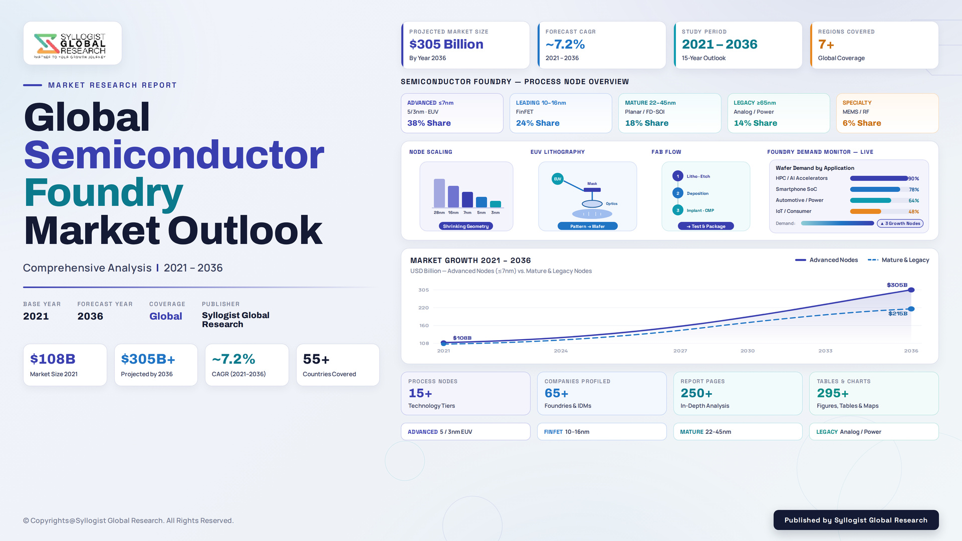
The global semiconductor foundry market is entering an unprecedented multi-year expansion cycle, propelled by accelerating AI accelerator demand, hyperscaler custom silicon proliferation, advanced packaging integration requirements, automotive semiconductor content growth, and the geopolitical restructuring of global semiconductor manufacturing capacity under US CHIPS Act, European Chips Act, Japanese semiconductor revitalization programs, and Asian self-sufficiency mandates. The market was valued at USD 145.8 billion in 2025 and is projected to reach USD 348.6 billion by 2034, advancing at a compound annual growth rate of 10.2% through the forecast period, supported by structural demand growth across leading-edge logic, accelerated capacity additions across mainstream and specialty nodes, and the rising share of advanced packaging revenue contributing to integrated foundry economics.
TSMC maintains the dominant position across the foundry industry with approximately 62% global foundry revenue share in 2025, anchored by exclusive 3 nm and forthcoming 2 nm production for Apple, NVIDIA, AMD, Qualcomm, MediaTek, and Broadcom, alongside the CoWoS advanced packaging franchise that supports nearly 100% of NVIDIA, AMD, and hyperscaler AI accelerator shipments. Samsung Foundry holds approximately 13% share with leading-edge 3 nm gate-all-around production at Pyeongtaek and forthcoming 2 nm capacity ramp, while Intel Foundry is targeting external customer share growth through 18A and 14A process nodes leveraging RibbonFET and PowerVia technologies at Ohio, Arizona, and Magdeburg fab sites. SMIC, GlobalFoundries, UMC, Tower Semiconductor, PSMC, VIS, Hua Hong, and Nexchip together cover the mainstream and specialty foundry segments, with combined revenue exceeding USD 32 billion in 2025 serving automotive, industrial, consumer, and communications applications.
AI accelerator demand has emerged as the single most consequential growth driver for leading-edge foundry revenue, with NVIDIA, AMD, Broadcom, Google, Microsoft, Amazon, and Meta collectively procuring leading-edge wafer capacity that contributes over 38% of TSMC 2025 revenue and is projected to exceed 48% by 2028 as Hopper, Blackwell, Rubin, MI300, MI400, and hyperscaler custom silicon programs scale. CoWoS, SoIC, and advanced packaging capacity at TSMC is doubling between 2024 and 2026 to over 70,000 wafers per month equivalent, with USD 18 billion of dedicated capital deployment supporting AI packaging capacity expansion. Automotive semiconductor foundry demand is simultaneously scaling rapidly, with TSMC, GlobalFoundries, UMC, Tower Semiconductor, and Nexchip serving automotive electronics content rising from approximately 1,400 USD per ICE vehicle to over 3,800 USD per fully electrified ADAS Level 2 platform.
Asia-Pacific dominates the global semiconductor foundry market with approximately 82% revenue share in 2025, anchored by Taiwan as the global leading-edge foundry hub generating over 65% of worldwide foundry output, followed by South Korea, China, and Japan as critical production geographies. China is the fastest growing regional market advancing at over 13.8% CAGR through 2034, supported by SMIC, Hua Hong Semiconductor, Nexchip, and emerging domestic foundries scaling mature and trailing-edge capacity under semiconductor self-sufficiency mandates and aggressive provincial subsidy frameworks. North America is rebuilding meaningful foundry share through CHIPS Act incentivized projects at TSMC Arizona, Intel Ohio, Samsung Taylor, and GlobalFoundries Malta, with combined committed capital expenditure exceeding USD 240 billion through 2030, while Europe is advancing capacity at TSMC Dresden, Intel Magdeburg, and STMicroelectronics-GlobalFoundries Crolles joint venture facilities targeting automotive and industrial end markets.
Key Drivers
AI Accelerator Demand, Hyperscaler Custom Silicon, and HPC Workload Growth Driving Leading-Edge Foundry Capacity Procurement
AI accelerator demand at NVIDIA, AMD, Broadcom, and hyperscaler custom silicon programs at Google, Microsoft, Amazon, and Meta is anchoring durable leading-edge foundry revenue growth, with AI-related wafer consumption contributing over 38% of TSMC 2025 revenue and projected to exceed 48% by 2028. Blackwell, Rubin, MI300, MI400, TPU, Trainium, Maia, and MTIA programs are collectively committing multi-billion USD long-term wafer agreements at 3 nm and 2 nm geometries, while CoWoS and advanced packaging capacity additions exceeding USD 18 billion of capex are reinforcing TSMC structural advantage across AI accelerator manufacturing through 2034.
CHIPS Act, European Chips Act, and Asian Self-Sufficiency Programs Accelerating Geographic Foundry Capacity Diversification
US CHIPS Act, European Chips Act, Japanese semiconductor revitalization programs, and Asian self-sufficiency mandates are accelerating geographic foundry capacity diversification, with TSMC Arizona, Intel Ohio, Samsung Taylor, GlobalFoundries Malta, TSMC Dresden, Intel Magdeburg, TSMC Kumamoto Phases 1 and 2, and Indian foundry initiatives collectively committing capital deployment exceeding USD 240 billion through 2030. These geographically distributed greenfield investments are reshaping global foundry capacity, customer routing, and trade architecture across leading-edge, mainstream, and specialty foundry segments.
Automotive Electrification, ADAS Adoption, and Rising Semiconductor Content per Vehicle Driving Mainstream and Specialty Foundry Growth
Automotive electrification, advanced driver assistance system adoption, and rising semiconductor content per vehicle are anchoring durable mainstream and specialty foundry demand growth, with automotive semiconductor content advancing from approximately 1,400 USD per ICE vehicle to over 3,800 USD per fully electrified ADAS Level 2 plus platform. Automotive foundry demand at TSMC, GlobalFoundries, UMC, Tower Semiconductor, and Nexchip is projected to advance at 11.4% CAGR through 2034, supported by microcontroller, power management, ADAS sensor, image sensor, and silicon carbide power device wafer procurement requirements.
Key Challenges
US Export Controls on Advanced Semiconductor Technology to China Reshaping Foundry Revenue Exposure and Trade Architecture
US Department of Commerce export controls covering advanced semiconductor manufacturing technology, sub-14 nm logic process IP, and advanced memory production tooling shipments to China are reshaping global foundry revenue exposure, market access, and trade architecture across leading-edge logic supply. TSMC, Samsung Foundry, and GlobalFoundries have disclosed material China revenue adjustments, while SMIC and emerging Chinese foundries are accelerating share capture across mainstream and trailing-edge categories as Chinese fabless customers aggressively qualify domestic foundry alternatives under self-sufficiency mandates.
Capital Intensity Escalation, Fab Construction Cost Inflation, and Greenfield Project Execution Risk Constraining Capacity Expansion Economics
Leading-edge fab construction costs have escalated materially, with greenfield 2 nm fab project capital intensity now exceeding USD 32 billion per facility and Arizona, Ohio, Taylor, Magdeburg, and Dresden projects collectively facing construction cost overruns of 18% to 35% relative to original budgets. Skilled engineering workforce shortages, equipment installation timeline extensions, qualification cycle complexity, and ecosystem partner readiness gaps are introducing greenfield project execution risk that complicates capacity ramp timelines, customer commitments, and capital allocation discipline across the foundry industry.
Mainstream and Trailing-Edge Capacity Overbuild, Chinese Foundry Expansion, and Pricing Compression Across Mature Nodes
Aggressive Chinese mainstream and trailing-edge foundry capacity expansion at SMIC, Hua Hong, Nexchip, and provincial-supported new entrants is creating localized capacity overbuild risks across 28 nm, 40 nm, 65 nm, and 90 nm process nodes, with global mature node capacity utilization declining below 78% across multiple quarters in 2024 and 2025. Pricing compression of 8% to 18% across mainstream foundry categories is pressuring margins at UMC, GlobalFoundries, Tower Semiconductor, PSMC, VIS, and DB HiTek, forcing strategic shifts toward specialty technologies, automotive qualification, and customer stickiness initiatives.
Market Segmentation
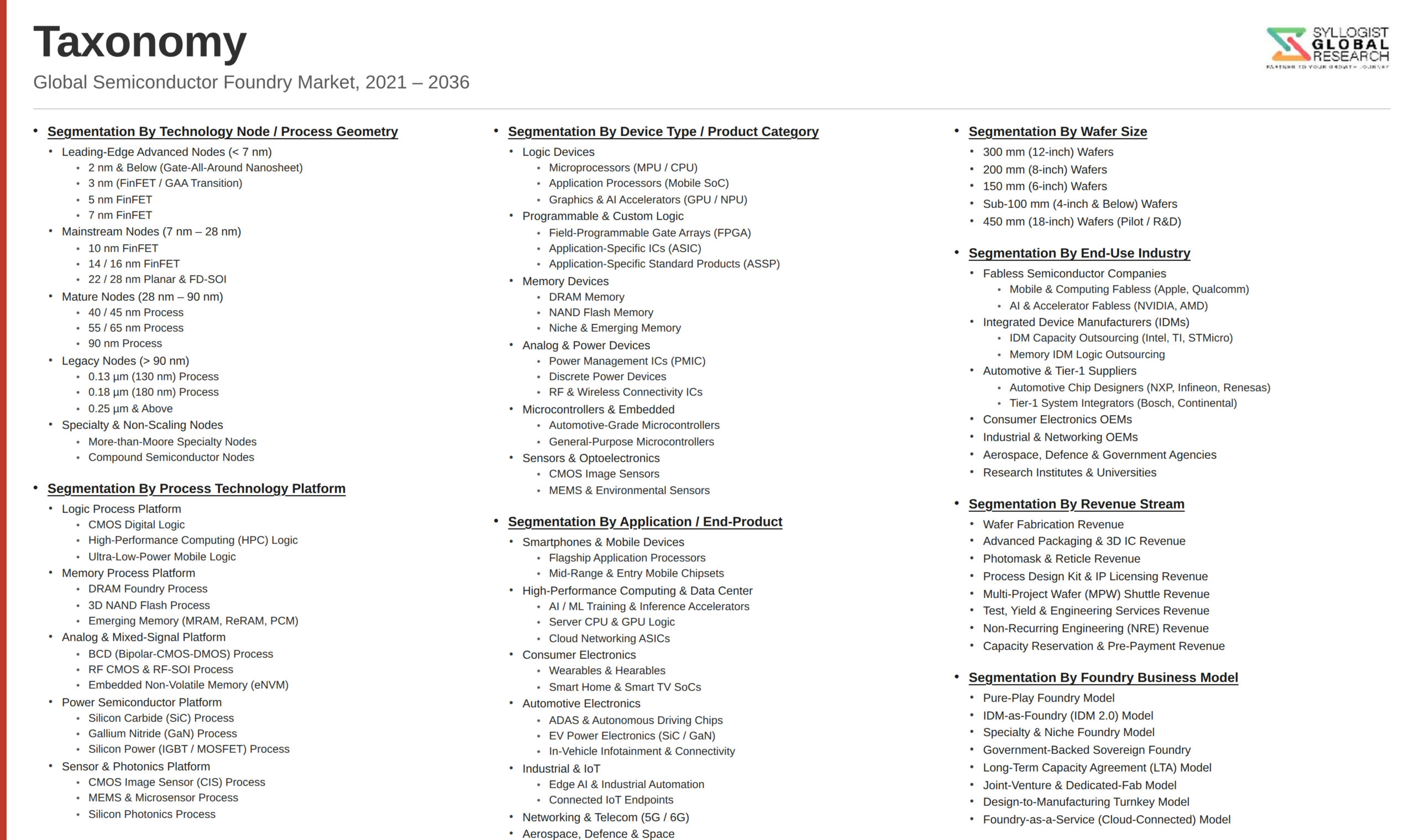
- Segmentation By Service Type
- Pure-Play Foundry Services
- IDM Foundry Services
- Multi-Project Wafer (MPW) Programs
- Mask Tooling and IP Licensing
- Advanced Packaging Services (CoWoS, SoIC, FOWLP, FOPLP)
- Specialty Process Foundry (RF SOI, BCD, eFlash, Image Sensor)
- Others
- Segmentation By Process Node
- Leading-Edge Logic (2 nm, 3 nm, 5 nm)
- Advanced Logic (7 nm, 10 nm)
- Mainstream Logic (14 nm, 16 nm, 22 nm, 28 nm)
- Mature Nodes (40 nm, 65 nm, 90 nm)
- Legacy Nodes (130 nm, 180 nm, and above)
- Compound Semiconductors (SiC, GaN, GaAs)
- Others
- Segmentation By Wafer Size
- 150 mm and Below
- 200 mm
- 300 mm
- Compound Semiconductor Wafers (100 mm, 150 mm, 200 mm)
- Others
- Segmentation By Application
- Smartphones and Mobile Devices
- AI Accelerators, GPUs, and HPC
- Data Center and Networking
- Automotive Electronics (ADAS, Powertrain, Infotainment)
- Industrial Automation and Robotics
- Consumer Electronics and IoT
- Communications (5G, RF, Optical)
- Power Semiconductors
- Image Sensors and Optoelectronics
- Others
- Segmentation By End User
- Fabless Semiconductor Companies
- Hyperscaler Custom Silicon Programs
- System OEMs
- Automotive Semiconductor Companies
- Telecom Equipment OEMs
- Defense, Aerospace, and Government
- Research Institutions
- Others
- Segmentation By Region
- Asia-Pacific (Taiwan, South Korea, China, Japan, Southeast Asia, India)
- North America
- Europe
- Middle East and Africa
- Latin America
All market revenues are presented in USD
Historical Year: 2021-2024 | Base Year: 2025 | Estimated Year: 2026 | Forecast Period: 2027-2034
Key Questions this Study Will Answer
- What is the total market valuation of the Global Semiconductor Foundry Market in 2025, projected through 2034, disaggregated by service type, process node, application, and end user, enabling foundry operators, fabless semiconductor companies, hyperscalers, and investors to identify the highest-growth opportunities and most durable revenue corridors across the foundry value chain?
- How is AI accelerator demand at NVIDIA, AMD, Broadcom, and hyperscaler custom silicon programs at Google, Microsoft, Amazon, and Meta reshaping leading-edge foundry capacity procurement, wafer pricing, and CoWoS advanced packaging allocation at TSMC, Samsung Foundry, and Intel Foundry through 2034?
- Which process nodes including 2 nm, 3 nm, 5 nm, 7 nm, 14 nm, 28 nm, 40 nm, 65 nm, and legacy nodes are generating the highest growth rates, and how are technology transitions reshaping competitive positioning across TSMC, Samsung Foundry, Intel Foundry, GlobalFoundries, SMIC, UMC, Tower Semiconductor, PSMC, VIS, Hua Hong, and Nexchip?
- How are US CHIPS Act, European Chips Act, Japanese semiconductor revitalization programs, and Asian self-sufficiency mandates driving geographic foundry capacity diversification across Arizona, Ohio, Taylor, Malta, Dresden, Magdeburg, Kumamoto, and emerging Indian foundry initiatives, and what regional demand patterns are emerging through 2034?
- How are US export controls on advanced semiconductor manufacturing technology shipments to China reshaping foundry supplier revenue exposure, market share dynamics, and competitive positioning, and how are SMIC, Hua Hong, Nexchip, and emerging Chinese foundries capturing share across mainstream and trailing-edge categories through 2034?
- How is automotive electrification, advanced driver assistance system adoption, and rising semiconductor content per vehicle reshaping mainstream and specialty foundry procurement across TSMC, GlobalFoundries, UMC, Tower Semiconductor, and Nexchip, and what application-level growth rates are projected through 2034?
- How is the competitive landscape structured among leading-edge foundries TSMC, Samsung Foundry, and Intel Foundry, mainstream operators GlobalFoundries, UMC, SMIC, PSMC, and VIS, and specialty foundries Tower Semiconductor, Hua Hong, DB HiTek, and Nexchip, and what partnership, capacity expansion, and customer retention strategies are reshaping market share dynamics through 2034?
- Product Definition
- Research Methodology
- Research Design & Framework
- Overall Research Approach: Descriptive, Exploratory & Quantitative Mixed-Method Design
- Market Definition & Scope Boundaries: What is Included and Excluded
- Segmentation Framework
- Key Research Assumptions & Limitations
- Secondary Research
- Primary Research Design & Execution
- Data Triangulation & Validation
- Market Sizing & Forecasting Methodology
- Competitive Intelligence Methodology
- Quality Assurance & Peer Review
- Definitions, Abbreviations & Data Notes
- Research Design & Framework
- Executive Summary
- Market Snapshot & Headline Numbers
- Key Findings & Research Highlights
- Market Dynamics
- Regional Market Summary
- Competitive Landscape Snapshot
- Technology & Innovation Highlights
- Market Dynamics
- Drivers
- Restraints
- Opportunities
- Challenges
- Porter’s Five Forces Analysis
- PESTLE Analysis
- Market Trends & Developments
- Emerging Trends
- Technological Developments
- Regulatory & Policy Changes
- Supply Chain & Sourcing Trends
- Manufacturing & Process Trends
- Investment & Funding Activity
- Sustainability & ESG Trends
- Risk Assessment Framework
- Capital Intensity, Fab Capex Cyclicality & Capacity Utilisation Risk
- Geopolitical, Export Control & Supply Chain Concentration Risk
- Technology Scaling, R&D Intensity & Node Transition Risk
- Customer Concentration, Demand Volatility & Inventory Correction Risk
- Equipment, Material & Critical Input Supply Risk
- Regulatory Framework & Standards
- Semiconductor Industry Standards & Process Qualification Frameworks (SEMI & JEDEC)
- Quality, Reliability & Automotive Qualification Standards (ISO, IATF 16949 & AEC-Q)
- Export Control, Trade Restriction & Technology Transfer Regulations
- Government Incentive, Subsidy & Domestic Manufacturing Policy Frameworks (CHIPS Acts & Equivalent)
- Environmental, Emissions, Water Use & Worker Safety Compliance Standards
- Global Semiconductor Foundry Market Outlook
- Market Size & Forecast by Value
- Market Size & Forecast by Volume (Wafer Shipments & Capacity, Thousand Wafers)
- Market Size & Forecast by Process Node
- Leading-Edge Nodes (Below 5 nm)
- 5 nm to 7 nm Nodes
- 7 nm to 10 nm Nodes
- 10 nm to 22 nm Nodes
- 22 nm to 45 nm Nodes
- 45 nm to 90 nm Nodes
- 90 nm to 180 nm Nodes
- 180 nm to 350 nm Nodes
- Above 350 nm (Legacy & Mature) Nodes
- Market Size & Forecast by Technology
- CMOS Logic Process Technology
- RF & RFCMOS Process Technology
- Analog & Mixed-Signal Process Technology
- Power (BCD, LDMOS & IGBT) Process Technology
- Embedded Non-Volatile Memory (eNVM) Process Technology
- MEMS & Sensor Process Technology
- Silicon-on-Insulator (SOI) Process Technology
- Compound Semiconductor (GaN, SiC & GaAs) Process Technology
- Other Specialty & Emerging Process Technologies
- Market Size & Forecast by Service Type
- Wafer Fabrication Services
- Mask Making & Photomask Services
- Design Enablement & IP Licensing Services
- Wafer-Level Test & Sort Services
- Advanced Packaging & Heterogeneous Integration Services
- Market Size & Forecast by Production Scale
- High-Volume Manufacturing (HVM) Fabs (Above 50,000 Wafers per Month)
- Medium-Volume Fabs (10,000 to 50,000 Wafers per Month)
- Low-Volume, Pilot & Specialty Fabs (Below 10,000 Wafers per Month)
- Market Size & Forecast by Application
- Smartphones & Consumer Electronics
- Computing, Data Center & High-Performance Computing (HPC)
- Automotive & Mobility Electronics
- Industrial & Power Electronics
- Communications, Networking & Wireless Infrastructure
- IoT, Wearables & Other Emerging Applications
- Market Size & Forecast by End-User
- Fabless Semiconductor Companies
- Integrated Device Manufacturers (IDMs)
- System OEMs & Hyperscalers
- Automotive & Industrial Electronics Companies
- Research Institutes & Other End-Users
- Market Size & Forecast by Sales Channel
- Direct Engagement & Long-Term Capacity Agreement
- Design Service & IP Partner Ecosystem
- Distributors & Aggregators
- Multi-Project Wafer (MPW) & Shuttle Programs
- North America Semiconductor Foundry Market Outlook
- Market Size & Forecast
- By Value
- By Volume (Wafer Shipments & Capacity, Thousand Wafers)
- By Process Node
- By Technology
- By Service Type
- By Production Scale
- By Application
- By End-User
- By Country
- By Sales Channel
- Europe Semiconductor Foundry Market Outlook
- Market Size & Forecast
- By Value
- By Volume (Wafer Shipments & Capacity, Thousand Wafers)
- By Process Node
- By Technology
- By Service Type
- By Production Scale
- By Application
- By End-User
- By Country
- By Sales Channel
- Asia-Pacific Semiconductor Foundry Market Outlook
- Market Size & Forecast
- By Value
- By Volume (Wafer Shipments & Capacity, Thousand Wafers)
- By Process Node
- By Technology
- By Service Type
- By Production Scale
- By Application
- By End-User
- By Country
- By Sales Channel
- Latin America Semiconductor Foundry Market Outlook
- Market Size & Forecast
- By Value
- By Volume (Wafer Shipments & Capacity, Thousand Wafers)
- By Process Node
- By Technology
- By Service Type
- By Production Scale
- By Application
- By End-User
- By Country
- By Sales Channel
- Middle East & Africa Semiconductor Foundry Market Outlook
- Market Size & Forecast
- By Value
- By Volume (Wafer Shipments & Capacity, Thousand Wafers)
- By Process Node
- By Technology
- By Service Type
- By Production Scale
- By Application
- By End-User
- By Country
- By Sales Channel
- Country-Wise* Semiconductor Foundry Market Outlook
- Market Size & Forecast
- By Value
- By Volume (Wafer Shipments & Capacity, Thousand Wafers)
- By Process Node
- By Technology
- By Service Type
- By Production Scale
- By Application
- By End-User
- By Country
- By Sales Channel
- *Countries Analyzed in the Syllogist Global Research Portfolio: United States, Canada, Mexico, Germany, France, United Kingdom, Netherlands, Spain, Italy, Norway, Sweden, China, Japan, India, Australia, South Korea, Singapore, Brazil, Chile, Saudi Arabia, UAE, Egypt, South Africa, Israel
- Technology Landscape & Innovation Analysis
- Leading-Edge Logic Scaling (FinFET, GAA & Nanosheet) Technology Deep-Dive
- Mature & Specialty Node Process Technology
- Advanced Lithography (EUV & High-NA EUV) Technology
- Advanced Packaging & Heterogeneous Integration (2.5D, 3D & Chiplet) Technology
- Compound Semiconductor & Wide-Bandgap (GaN & SiC) Process Technology
- Design Enablement, PDK, EDA & IP Ecosystem Technology
- Yield Enhancement, Defect Inspection & Smart Manufacturing Technology
- Patent & IP Landscape in Semiconductor Foundry Technologies
- Value Chain & Supply Chain Analysis
- Silicon Wafer, Substrate & Raw Material Supply Chain
- Semiconductor Manufacturing Equipment (Lithography, Etch & Deposition) Supply Chain
- Specialty Gases, Chemicals & Photoresist Supply Chain
- Photomask, EDA & Design IP Supply Chain
- Foundry Fabrication, Process Integration & Operations Landscape
- OSAT, Packaging & Test Partner Channel
- Reclaim, Recycling & Circular Economy
- Pricing Analysis
- Leading-Edge Node Wafer Pricing and Cost Analysis
- Mature & Legacy Node Wafer Pricing and Cost Analysis
- Specialty Process (RF, Power & Analog) Wafer Pricing Analysis
- Mask Set, NRE & Design Enablement Cost Analysis
- Foundry Capacity, Capex & Wafer-Cost Structure Analysis
- Total Foundry Economics: Cost-per-Transistor and Yield-Adjusted Wafer-Cost Optimisation Analysis
- Sustainability & Environmental Analysis
- Lifecycle Assessment (LCA) of Semiconductor Manufacturing: Carbon Footprint, Energy & Water Intensity Across Process Nodes
- Carbon Neutrality & Net Zero Contribution: Pathway to Renewable-Powered Fabs
- Water Stewardship, Recycling & Resource Efficiency Contribution
- Environmental Compliance, PFAS, Process Emissions & Chemical Waste Consideration in Fab Operations
- Regulatory-Driven Sustainability, SDG 9 (Industry & Innovation) & SDG 12 (Responsible Consumption) Alignment & Green Finance Eligibility
- Competitive Landscape
- Market Structure & Concentration
- Market Consolidation Level (Fragmented vs. Consolidated by Process Node & Geography)
- Top 10 Players Market Share
- HHI (Herfindahl-Hirschman Index) Concentration Analysis
- Competitive Intensity Map by Process Node, Technology & Geography
- Player Classification
- Leading-Edge Pure-Play Foundries
- Mature & Specialty Node Pure-Play Foundries
- IDM Foundries & IDM 2.0 Players
- Memory-Focused Foundry & IDM Players
- Compound Semiconductor & Wide-Bandgap Foundries
- Analog, RF & Power Specialty Foundries
- MEMS & Sensor Foundries
- Emerging & Regional Foundry Entrants
- Competitive Analysis Frameworks
- Market Share Analysis by Process Node, Technology & Region
- Company Profile
- Company Overview & Headquarters
- Foundry Services & Process Technology Portfolio
- Key Customer Relationships & Reference Engagements
- Manufacturing Footprint & Wafer Capacity
- Revenue (Foundry Segment) & Backlog
- Technology Differentiators & IP
- Key Strategic Partnerships, JVs & M&A Activity
- Recent Developments (Fab Expansion, Capacity Announcements, Node Launches)
- SWOT Analysis
- Strategic Focus Areas & Roadmap
- Competitive Positioning Map (Technology Capability vs. Market Penetration)
- Key Company Profiles
- Market Structure & Concentration
- Technology Landscape & Innovation Analysis
- Strategic Output
- Market Opportunity Matrix: By Process Node, Technology, Application, End-User & Geography
- White Space Opportunity Analysis
- Strategic Recommendations
- Product Portfolio & Technology Investment Strategy
- Manufacturing & Operational Excellence Strategy
- Geographic Expansion & Localisation Strategy
- Customer & End-User Engagement Strategy
- Partnership, M&A & Ecosystem Strategy
- Sustainability & Circular Economy Strategy
- Risk Mitigation & Future Roadmap
- Strategic Priority Matrix & Roadmap
- Near-term (2025-2028)
- Mid-term (2029-2032)
- Long-term (2033-2037)
- Strategic Output
- Market Size & Forecast
- Market Size & Forecast
- Market Size & Forecast
- Market Size & Forecast
- Market Size & Forecast
- Market Size & Forecast