Market Definition
The Global Semiconductor Process Chemicals Market encompasses the development, formulation, manufacturing, distribution, and application of high-purity chemical compounds and specialty chemical solutions used across the complete semiconductor fabrication value chain, from front-end wafer processing operations including photolithography, chemical mechanical planarization, wet cleaning and etching, thermal oxidation, and thin film deposition, through to back-end packaging, assembly, and wafer-level packaging processes that collectively define the chemical inputs required for the production of integrated circuits, memory devices, logic chips, power semiconductors, compound semiconductors, and optoelectronic components manufactured on silicon, silicon carbide, gallium nitride, and III-V compound semiconductor substrates. Semiconductor process chemicals include photoresists and associated ancillary chemicals such as anti-reflective coatings, developers, and photoresist strippers; wet process chemicals encompassing ultrapure hydrofluoric acid, sulfuric acid, hydrogen peroxide, ammonium hydroxide, and phosphoric acid; chemical mechanical planarization slurries and post-CMP cleaning solutions; chemical vapor deposition precursors and atomic layer deposition source chemicals; ion implantation dopant gases; and specialty cleaning and surface conditioning agents whose purity specifications are measured in parts-per-trillion metallic contamination levels. The market is defined by extraordinary purity and consistency requirements imposed by advanced logic and memory node fabrication, where trace contamination at the sub-parts-per-trillion level can compromise device yield across entire wafer lots. Key participants include integrated chemical manufacturers, specialty chemical formulators, electronic-grade gas suppliers, chemical delivery system providers, semiconductor original equipment manufacturers, and fabrication facility operators whose process specifications govern formulation and supply across major global wafer fabrication hubs in Asia-Pacific, North America, and Europe.
Market Insights
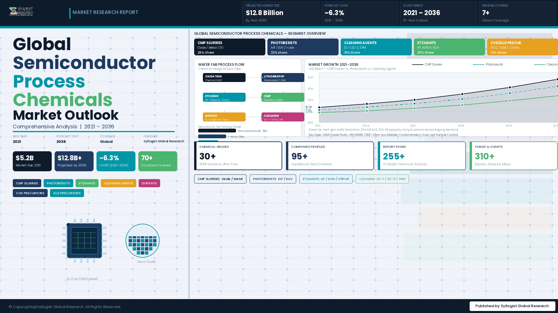
The global semiconductor process chemicals market was valued at approximately USD 7.8 billion in 2025 and is projected to reach USD 12.6 billion by 2034, advancing at a compound annual growth rate of 5.5% over the forecast period from 2027 to 2034. The primary growth engine is the continuous advancement of semiconductor process nodes, where each technology generation requires new chemical formulations, higher purity grades, and novel precursor chemistries that command significantly higher average selling prices than their predecessors. The transition to gate-all-around nanosheet transistor architectures at 3-nanometer and 2-nanometer process nodes has introduced new requirements for selective etch chemistries, conformal deposition precursors, and high-selectivity CMP slurries, driving a structural uplift in process chemical value intensity per wafer start at leading-edge fabrication facilities that is expected to persist through the forecast period as node transitions continue toward 1-nanometer and angstrom-class technologies.
Advanced packaging and heterogeneous integration represent the fastest-growing application segment within semiconductor process chemicals, driven by industry adoption of 2.5D and 3D integrated circuit packaging architectures that require specialty dielectric deposition precursors, electroplating chemistries, and cleaning solutions formulated for through-silicon via and redistribution layer processes. The compound semiconductor segment encompassing silicon carbide and gallium nitride device fabrication for electric vehicle powertrains and grid-scale power conversion is generating incremental demand for process chemicals tailored to wide-bandgap substrates, advancing at approximately 14.2% annually. Memory technology transitions, including the scaling of NAND flash to 300-layer-plus stacks and the introduction of high-bandwidth memory for artificial intelligence accelerators, are simultaneously expanding the consumption intensity of specialty wet chemicals, CMP slurries, and cleaning formulations per unit of memory device output across leading memory fabrication facilities.
Asia-Pacific accounts for approximately 68% of global wafer fabrication capacity in 2025, anchored by Taiwan, South Korea, Japan, and China, whose collective semiconductor manufacturing output encompasses the majority of global leading-edge logic, DRAM, NAND flash, and power device production. Taiwan remains the single most significant national market for advanced logic process chemicals owing to the concentration of the world’s most advanced foundry capacity, while South Korea generates the largest demand pool for CMP slurries and wet cleaning chemicals on a wafer-area-normalized basis. China’s domestic semiconductor process chemicals market exhibits bifurcated dynamics, with mature-node fabrication capacity expanding rapidly and generating growing demand for established chemical grades, while access to process chemicals for sub-7-nanometer logic fabrication remains constrained by export control frameworks maintained by multiple technology-exporting nations.
The semiconductor process chemicals supply chain is characterized by extreme supplier concentration in technically differentiated product categories, with photoresists for extreme ultraviolet lithography applications served by a limited number of specialty manufacturers whose formulations represent decades of proprietary development. Geopolitical supply chain risk awareness has prompted leading semiconductor manufacturers to intensify supplier diversification programs, regional supply localization initiatives, and strategic chemical inventory buffer stocking. Government-sponsored programs in the United States, European Union, Japan, and South Korea are providing direct investment support for domestic process chemical manufacturing capacity, with cumulative government-directed incentives for semiconductor supply chain localization estimated at approximately USD 4.3 billion across these jurisdictions between 2023 and 2025, creating a structural tailwind for regional chemical supply development over the forecast period.
Key Drivers
Accelerating Node Transitions and Rising Chemical Intensity per Wafer Start at Leading-Edge Logic and Memory Fabrication Nodes
The relentless advancement of semiconductor device architectures to smaller, more complex process nodes is generating a sustained and structurally expanding demand for novel process chemicals whose formulation complexity, purity requirements, and per-unit value are substantially higher than the commodity chemical grades they displace from the fabrication process sequence. Gate-all-around nanosheet transistor architectures at 3-nanometer and 2-nanometer process nodes require entirely new selective etch chemistries capable of removing gate dielectric and channel materials with atomic-level precision without attacking adjacent structures, conformal atomic layer deposition precursors for high-k gate dielectric and metal gate fill applications, and CMP slurries formulated to planarize novel metal interconnect and dielectric material combinations with defect densities compatible with advanced device yield requirements. The transition from conventional to backside power delivery network architectures introduces an additional back-end wafer thinning, through-silicon via formation, and dielectric deposition sequence that further increases process chemical consumption per wafer start. Each successive node transition at the leading edge of fabrication technology generates a qualification and adoption cycle for new chemical formulations in which specialty chemical suppliers can establish technically differentiated, high-margin supply positions before cost-reduction pressures develop, sustaining above-average revenue and margin growth for technically capable suppliers through the forecast period to 2034.
Semiconductor Fabrication Capacity Expansion Programs Across Asia-Pacific, North America, and Europe Generating Multi-Year Process Chemical Demand Commitments
The largest coordinated expansion of semiconductor fabrication capacity in industry history is underway across Asia-Pacific, North America, and Europe, driven by government industrial policy investments and national security imperatives that have collectively committed significant capital to the construction and equipping of new wafer fabrication facilities whose process chemical supply requirements will generate sustained, multi-year demand commitments for qualified specialty chemical suppliers. New advanced logic fab projects in the United States, Japan, and Europe are installing significant leading-edge fabrication capacity at 3-nanometer to 5-nanometer technology nodes, where the combined annual consumption of process chemicals at a single leading-edge fab can represent approximately USD 80 million to USD 120 million in procurement value. Mature-node and specialty semiconductor fab expansions targeting automotive, industrial, and analog device production are simultaneously expanding globally, creating broad-based demand growth for wet chemicals, photoresists, and CMP consumables across a wider range of technology nodes than leading-edge expansion alone would generate. The long qualification lead times of 18 to 36 months required for process chemical certification at new fabs create durable supplier incumbency advantages for qualified chemical suppliers and generate predictable revenue streams tied to fab construction and ramp schedules extending through 2030 and beyond.
Extreme Ultraviolet Lithography Adoption and Next-Generation Patterning Requirements Creating Structurally High-Value Photoresist and Ancillary Chemistry Demand
The broad adoption of extreme ultraviolet lithography across leading-edge logic and DRAM fabrication is creating a structural transition in photoresist and ancillary chemistry requirements that generates meaningfully higher average selling prices and more technically complex supply relationships relative to the ArF immersion lithography generation it progressively displaces. Extreme ultraviolet photoresists, including both chemically amplified resist and metal oxide resist platforms under active commercialization, must simultaneously satisfy photon absorption efficiency, resolution, line edge roughness, and etch resistance requirements at 13.5-nanometer exposure wavelength that are fundamentally more demanding than the corresponding specifications for ArF immersion photoresists operating at 193-nanometer wavelength. High-numerical-aperture extreme ultraviolet lithography, entering pilot production use at leading-edge foundries, introduces further requirements for thinner resist films, enhanced underlayer chemistries, and novel anti-reflective coating formulations that require additional qualification cycles and generate a further uplift in photochemistry system value per exposure. The photomask cleaning chemicals, rinse solutions, and defect detection reagents required for extreme ultraviolet mask qualification and maintenance represent a related high-value chemical sub-segment growing in direct proportion to EUV tool installation rates at leading-edge fabrication facilities globally.
Key Challenges
Ultra-High Purity Requirements and the Escalating Cost and Duration of Chemical Qualification at Leading-Edge Process Nodes
The qualification of process chemicals for use at sub-5-nanometer logic and advanced DRAM process nodes represents one of the most technically demanding and time-intensive supplier certification processes in any manufacturing industry, requiring chemical suppliers to demonstrate metallic contamination levels at or below parts-per-trillion thresholds across dozens of trace elements, particle counts below single-digit particles per milliliter at sizes down to 20 nanometers, and process performance consistency within specifications that have become progressively tighter with each technology node generation. Full chemical qualification cycles at advanced logic nodes now commonly require 18 to 36 months from initial sample submission to production supply authorization, involving joint development investment by the chemical supplier that can reach USD 5 million to USD 15 million per product across analytical method development, formulation optimization, and process performance demonstration programs. These qualification barriers simultaneously protect incumbent chemical suppliers with established process approvals and create substantial market entry obstacles for new entrants, constraining competitive dynamics and limiting the ability of semiconductor manufacturers to diversify their chemical supply base in technically sensitive product categories. The escalating purity specifications associated with each successive node transition impose continuous reinvestment requirements on chemical manufacturers to upgrade analytical capabilities, refine manufacturing process controls, and redesign chemical delivery systems, generating persistent capital intensity that compresses margins in all but the most technically differentiated product categories.
Geopolitical Export Controls and Supply Chain Fragmentation Disrupting Chemical Supply Security for Globally Distributed Semiconductor Manufacturers
The semiconductor process chemicals market has become deeply embedded in geopolitical competition over semiconductor technology leadership, with export control measures implemented by the United States, Japan, the Netherlands, and other technology-exporting nations progressively restricting the supply of advanced photoresists, specialty etch chemicals, and high-purity precursor materials to semiconductor manufacturers in controlled destination countries, creating supply chain fragmentation dynamics that impose compliance costs and supply security risks on both chemical suppliers and their customers. Compliance with overlapping national export control frameworks requires process chemical suppliers to maintain detailed end-use tracking systems, conduct customer due diligence programs, and obtain individual export licenses for controlled chemical categories, imposing administrative burden that is particularly challenging for smaller specialty chemical suppliers with limited regulatory compliance infrastructure. Semiconductor manufacturers operating globally must manage the risk that export control expansions may interrupt the supply of currently approved chemical categories with limited or no qualified alternative supply, motivating substantial investment in chemical inventory buffer building, alternative supplier qualification programs, and domestic chemical supply development that collectively increase working capital requirements and procurement management complexity. The progressive bifurcation of the global semiconductor supply chain into partially separate technology ecosystems is creating divergent chemical specification roadmaps that may reduce scale economies available to chemical suppliers attempting to serve both ecosystem segments simultaneously.
Raw Material Supply Concentration, Specialty Precursor Scarcity, and Environmental Compliance Cost Escalation in Process Chemical Manufacturing
Semiconductor process chemical manufacturing depends on a narrow set of ultra-high-purity precursor raw materials whose global production is concentrated in a small number of facilities, creating structural supply vulnerability to production disruptions, natural disasters, or export restrictions at individual manufacturing sites, a risk profile that has been demonstrated repeatedly by historical supply incidents affecting hydrofluoric acid, neon gas, and specialty organometallic precursor supply chains. The precursor supply chain for advanced deposition chemistries, including hafnium, zirconium, and ruthenium organometallic precursors for high-k dielectric and metal gate applications, and cobalt and tungsten carbonyl precursors for next-generation interconnect fill processes, is supplied by a small number of synthetic chemistry specialists whose manufacturing scale is limited by the technical complexity and hazardous nature of organometallic synthesis, constraining the pace at which precursor supply can be expanded to meet growing demand from fab capacity expansion programs. Environmental and safety regulations governing the manufacture, transport, handling, and disposal of hazardous process chemicals including hydrofluoric acid, sulfuric acid, hydrogen peroxide, and specialty etch gases are becoming progressively more stringent across major chemical manufacturing jurisdictions, imposing compliance investment requirements and operational cost increases that compress margins in commodity chemical categories. Water treatment and waste chemical disposal requirements at semiconductor-grade chemical manufacturing facilities are generating capital investment demands that disproportionately burden smaller specialty manufacturers and create consolidation pressure within the process chemical supply base.
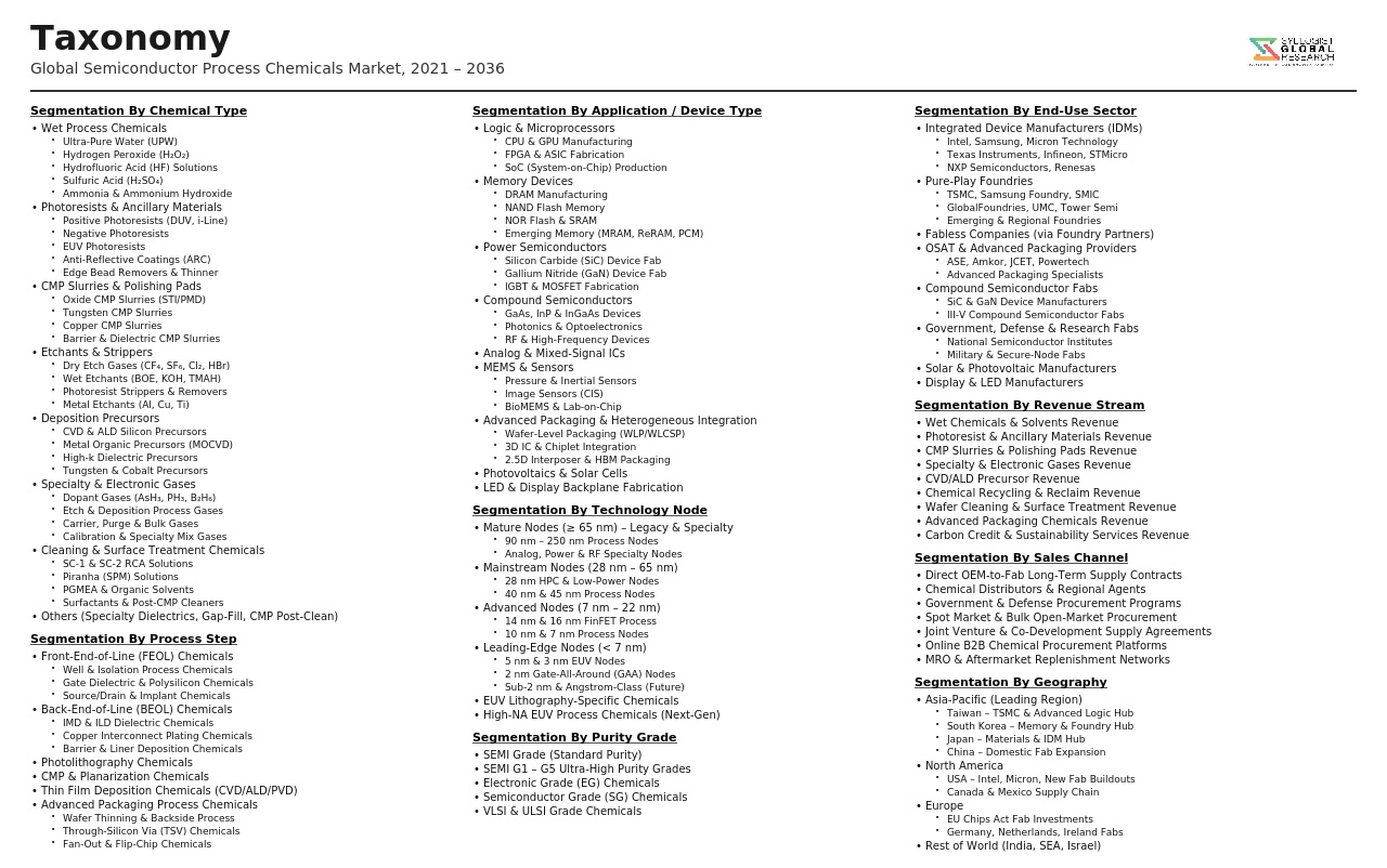
Market Segmentation
- Segmentation By Chemical Type
- Wet Process Chemicals (Acids, Bases, and Solvents)
- Photoresists (ArF Immersion, EUV Chemically Amplified, Metal Oxide, and g/i-Line)
- Chemical Mechanical Planarization (CMP) Slurries
- CMP Post-Polish Cleaning and Brush Cleaning Solutions
- Anti-Reflective Coatings and Photoresist Ancillary Chemistries
- Atomic Layer Deposition and CVD Precursor Chemicals
- Specialty Etch Gases and Plasma Process Chemistries
- Electroplating and Electroless Plating Chemistries
- Others
- Segmentation By Process Step
- Photolithography and Pattern Definition
- Chemical Mechanical Planarization
- Wet Cleaning and Surface Preparation
- Wet and Dry Etching
- Thin Film Deposition (CVD, ALD, and PVD)
- Ion Implantation
- Advanced Packaging and Wafer-Level Packaging
- Others
- Segmentation By Technology Node
- Legacy Nodes (Above 28 nm)
- Mature Nodes (28 nm to 7 nm)
- Advanced Nodes (7 nm to 3 nm)
- Leading-Edge Nodes (Below 3 nm, including Gate-All-Around and Angstrom-Class)
- Segmentation By Semiconductor Device Type
- Logic and Microprocessors
- DRAM Memory
- NAND Flash Memory
- Power Semiconductors (Silicon)
- Silicon Carbide (SiC) Power Devices
- Gallium Nitride (GaN) Devices
- Compound Semiconductors and III-V Devices
- Analog and Mixed-Signal Semiconductors
- MEMS and Sensors
- Others
- Segmentation By Application
- Front-End-of-Line Wafer Fabrication
- Back-End-of-Line Wafer Fabrication
- Advanced Packaging and Heterogeneous Integration
- Photomask Manufacturing and Cleaning
- Substrate and Printed Circuit Board Manufacturing
- Others
- Segmentation By End User
- Integrated Device Manufacturers (IDMs)
- Pure-Play Foundries
- Memory Manufacturers (DRAM and NAND Flash)
- Compound Semiconductor Manufacturers
- Advanced Packaging and OSAT Providers
- Others
- Segmentation By Purity Grade
- SEMI-Grade (G1 to G5)
- Electronic Grade
- Ultra-High Purity (UHP) Grade
- Others
- Segmentation By Sales Channel
- Direct Supply to Semiconductor Fabrication Facilities
- Chemical Distributors and Wholesalers
- Chemical Delivery System Integrators
- Others
- Segmentation By Region
- North America
- Europe
- Asia-Pacific
- Middle East and Africa
- Latin America
All market revenues are presented in USD
Historical Year: 2021-2024 | Base Year: 2025 | Estimated Year: 2026 | Forecast Period: 2027-2034
Key Questions this Study Will Answer
- What is the total global market valuation of the Semiconductor Process Chemicals Market in the base year 2025, and what is the projected market size and compound annual growth rate through 2034, disaggregated by chemical type, photoresist, wet process chemicals, CMP slurries, and deposition precursors, and by application, front-end wafer fabrication, back-end processing, and advanced packaging, to enable chemical manufacturers, semiconductor fabricators, materials investors, and supply chain strategists to identify which product categories and application segments will generate the highest absolute revenue and the most durable growth trajectory across the forecast period in the context of accelerating node transitions and expanding fab capacity?
- How is the industry-wide transition to extreme ultraviolet lithography and high-numerical-aperture EUV expected to reshape the photoresist and photochemistry ancillary market through 2034, including the relative adoption trajectories of chemically amplified resist and metal oxide resist platforms, the per-wafer photochemistry cost implications for leading-edge logic and DRAM manufacturers, and which specialty chemical suppliers are best positioned to capture the technology upgrade spending cycle associated with EUV process adoption at scale across Taiwan, South Korea, the United States, and Japan?
- What is the projected market size, growth rate, and competitive structure of the compound semiconductor process chemicals segment encompassing silicon carbide, gallium nitride, and III-V device fabrication through 2034, which process chemical categories, specialty etch gases, surface passivation chemistries, and epitaxial deposition precursors, are generating the highest growth rates, and how are electric vehicle powertrain adoption and power grid modernization investment translating into sustained procurement demand for wide-bandgap semiconductor process chemicals at established and newly constructed compound semiconductor fabrication facilities globally?
- How are geopolitical export control frameworks and supply chain localization policies across the United States, European Union, Japan, South Korea, and China expected to reshape the competitive structure, supplier geography, and pricing dynamics of the semiconductor process chemicals market through 2034, and what are the investment implications for chemical manufacturers pursuing regional supply development, for semiconductor manufacturers managing chemical supply security, and for government programs directing industrial policy capital toward domestic semiconductor materials manufacturing capacity?
- Who are the leading specialty chemical manufacturers, wet process chemical suppliers, photoresist developers, CMP slurry formulators, and deposition precursor producers currently defining the competitive landscape of the global semiconductor process chemicals market, and what are their respective product portfolios across technology nodes and chemical categories, manufacturing footprint and capacity expansion strategies, customer qualification status at leading-edge fabrication facilities, technology development roadmaps for next-generation EUV and sub-2-nanometer node chemistries, and strategic responses to the geopolitical supply chain fragmentation reshaping global semiconductor materials sourcing?
- Product Definition
- Research Methodology
- Research Design & Framework
- Overall Research Approach: Descriptive, Exploratory & Quantitative Mixed-Method Design
- Market Definition & Scope Boundaries: What is Included and Excluded
- Segmentation Framework
- Key Research Assumptions & Limitations
- Secondary Research
- Primary Research Design & Execution
- Data Triangulation & Validation
- Market Sizing & Forecasting Methodology
- Competitive Intelligence Methodology
- Quality Assurance & Peer Review
- Definitions, Abbreviations & Data Notes
- Research Design & Framework
- Executive Summary
- Market Snapshot & Headline Numbers
- Key Findings & Research Highlights
- Market Dynamics
- Regional Market Summary
- Competitive Landscape Snapshot
- Technology & Innovation Highlights
- Market Dynamics
- Drivers
- Restraints
- Opportunities
- Challenges
- Porter’s Five Forces Analysis
- PESTLE Analysis
- Market Trends & Developments
- Emerging Trends
- Technological Developments
- Regulatory & Policy Changes
- Supply Chain & Sourcing Trends
- Manufacturing & Process Trends
- Investment & Funding Activity
- Sustainability & ESG Trends
- Risk Assessment Framework
- Raw Material Availability, Geopolitical Supply Risk & Critical Mineral Dependency
- Export Controls, Trade Restrictions & Technology Decoupling Risk
- Chemical Hazard, Handling, Storage & Environmental Liability Risk
- Semiconductor Fab Demand Cyclicality, Capacity Utilisation & Volume Risk
- Regulatory, PFAS Phase-Out, REACH & Cross-Border Compliance Risk
- Regulatory Framework & Standards
- Semiconductor Chemical Purity Standards, SEMI Standards (SEMI C-Series) & International Specifications for Ultra-High-Purity Chemicals
- Chemical Safety Regulations: REACH, GHS/SDS, TSCA & Hazardous Substance Control Frameworks Applicable to Semiconductor Process Chemicals
- PFAS and Fluorinated Compound Regulation: EU PFAS Restriction Proposals, US EPA PFAS Action Plan & Implications for Semiconductor Photoresists and Etchants
- Environmental Permitting, Air Emission Controls, Wastewater Discharge Standards & Waste Management Regulations for Semiconductor Chemical Users
- Export Control Regimes (EAR, Wassenaar Arrangement) & Strategic Trade Policy Applicable to Advanced Semiconductor Chemicals and Precursors
- Global Semiconductor Process Chemicals Market Outlook
- Market Size & Forecast by Value
- Market Size & Forecast by Volume (Metric Tons)
- Market Size & Forecast by Chemical Type
- Photoresists (EUV, DUV ArF Immersion, DUV KrF, i-line and g-line Resists)
- Photoresist Ancillaries (Developers, Strippers, Anti-Reflective Coatings and Topcoats)
- CMP Slurries (Oxide, Copper, Tungsten, STI and Low-k Dielectric Slurries)
- CMP Pads and Pad Conditioners
- Wet Cleaning and Surface Preparation Chemicals (SC-1, SC-2, SPM, DHF and Ozone-Based Chemistries)
- Wet Etch Chemicals (HF, HNO3, H3PO4, KOH and TMAH-Based Etchants)
- Solvents (IPA, NMP, PGMEA and Other Semiconductor-Grade Solvents)
- Chemical Vapour Deposition (CVD) and Atomic Layer Deposition (ALD) Precursors
- Dopant Chemicals and Ion Implant Source Chemicals
- Specialty Chemicals for Advanced Packaging and 3D Integration
- Market Size & Forecast by Process Step
- Lithography and Patterning
- Etching (Wet Etch and Post-Etch Residue Removal)
- Chemical Mechanical Planarization (CMP)
- Thin Film Deposition (CVD, ALD and PVD-Related Chemistries)
- Cleaning and Surface Preparation
- Doping and Ion Implantation
- Packaging, Interconnect and Assembly
- Market Size & Forecast by Application
- Front-End-of-Line (FEOL) Wafer Processing
- Back-End-of-Line (BEOL) Metallisation and Interconnect
- Advanced Packaging (Flip Chip, Wafer-Level Packaging and 2.5D/3D Integration)
- Market Size & Forecast by Technology Node
- Leading Edge (Below 7nm, EUV-Enabled)
- Advanced (7nm to 28nm)
- Mainstream (28nm to 90nm)
- Mature (Above 90nm)
- Market Size & Forecast by End-Use Segment
- Logic and Microprocessors (CPU, GPU and AI Accelerators)
- Memory (DRAM)
- Memory (NAND Flash and 3D NAND)
- Analog, Mixed-Signal and Power Semiconductors
- RF, Communications and Photonics
- MEMS, Sensors and Specialty Devices
- Market Size & Forecast by Wafer Size
- 150mm (6-Inch)
- 200mm (8-Inch)
- 300mm (12-Inch)
- Market Size & Forecast by Sales Channel
- Direct Supply to Integrated Device Manufacturers (IDMs)
- Supply to Pure-Play Foundries and OSATs
- Specialty Chemical Distributors and Trading Houses
- OEM and Long-Term Supply Agreement Channels
- North America Semiconductor Process Chemicals Market Outlook
- Market Size & Forecast
- By Value
- By Volume (Metric Tons)
- By Chemical Type
- By Process Step
- By Application
- By Technology Node
- By End-Use Segment
- By Wafer Size
- By Country
- By Sales Channel
- Market Size & Forecast
- Europe Semiconductor Process Chemicals Market Outlook
- Market Size & Forecast
- By Value
- By Volume (Metric Tons)
- By Chemical Type
- By Process Step
- By Application
- By Technology Node
- By End-Use Segment
- By Wafer Size
- By Country
- By Sales Channel
- Market Size & Forecast
- Asia-Pacific Semiconductor Process Chemicals Market Outlook
- Market Size & Forecast
- By Value
- By Volume (Metric Tons)
- By Chemical Type
- By Process Step
- By Application
- By Technology Node
- By End-Use Segment
- By Wafer Size
- By Country
- By Sales Channel
- Market Size & Forecast
- Latin America Semiconductor Process Chemicals Market Outlook
- Market Size & Forecast
- By Value
- By Volume (Metric Tons)
- By Chemical Type
- By Process Step
- By Application
- By Technology Node
- By End-Use Segment
- By Wafer Size
- By Country
- By Sales Channel
- Market Size & Forecast
- Middle East & Africa Semiconductor Process Chemicals Market Outlook
- Market Size & Forecast
- By Value
- By Volume (Metric Tons)
- By Chemical Type
- By Process Step
- By Application
- By Technology Node
- By End-Use Segment
- By Wafer Size
- By Country
- By Sales Channel
- Market Size & Forecast
- Country-Wise* Semiconductor Process Chemicals Market Outlook
- Market Size & Forecast
- By Value
- By Volume (Metric Tons)
- By Chemical Type
- By Process Step
- By Application
- By Technology Node
- By End-Use Segment
- By Wafer Size
- By Country
- By Sales Channel
- Market Size & Forecast
- *Countries Analyzed in the Syllogist Global Research Portfolio: United States, Canada, Mexico, Germany, France, United Kingdom, Netherlands, Belgium, Japan, South Korea, Taiwan, China, Singapore, Malaysia, Israel, India, Australia, Brazil, Saudi Arabia, UAE, Ireland
- Technology Landscape & Innovation Analysis
- EUV and Next-Generation Photoresist Technology Deep-Dive
- CMP Slurry and Pad Technology for Advanced Nodes
- Atomic Layer Deposition (ALD) Precursor Chemistry Innovations
- Low-k and Ultra-Low-k Dielectric Chemical Technologies
- Advanced Cleaning Chemistry for Sub-5nm Nodes
- Green and Sustainable Chemistry Innovations in Semiconductor Processing
- Digital and AI-Assisted Chemical Process Optimisation Platforms
- Patent & IP Landscape in Semiconductor Process Chemical Technologies
- Value Chain & Supply Chain Analysis
- Raw Material and Precursor Chemical Supply Chain
- Photoresist and Photochemical Manufacturing Supply Chain
- CMP Slurry and Abrasive Materials Supply Chain
- Ultra-Pure Acids, Solvents and Wet Chemical Supply Chain
- CVD and ALD Precursor Manufacturing and Distribution
- Chemical Blending, Formulation and Quality Assurance
- Logistics, Handling and On-Site Chemical Management at Fabs
- Waste Treatment, Chemical Recovery and Circular Economy
- Pricing Analysis
- Photoresist and EUV Resist Pricing Trends and Cost Structure
- CMP Slurry Pricing Analysis by Planarisation Application
- Wet Chemical (Acids and Solvents) Spot and Contract Pricing
- CVD and ALD Precursor Pricing and Volume Discount Structure
- Total Cost of Ownership (TCO) Analysis: Chemical Cost Per Wafer Pass
- Pricing Pressure, Negotiation Dynamics and Supply Agreement Structures
- Sustainability & Environmental Analysis
- Lifecycle Assessment (LCA) of Semiconductor Process Chemicals: Carbon Footprint, Water Intensity and Hazardous Waste Generation Across Chemical Categories
- Fluorinated Compound (PFAS) Regulation and Phase-Out Pathway for Semiconductor Chemistries
- Water Recycling, Chemical Reclaim and Zero-Liquid-Discharge Initiatives at Semiconductor Fabs
- Green Chemistry, Bio-Based Alternatives and Solvent Substitution Programmes
- Regulatory-Driven Sustainability, REACH, RoHS and ESG Alignment in Semiconductor Chemical Supply Chains
- Competitive Landscape
- Market Structure & Concentration
- Market Consolidation Level (Fragmented vs. Consolidated by Chemical Type and Geography)
- Top 10 Players Market Share
- HHI (Herfindahl-Hirschman Index) Concentration Analysis
- Competitive Intensity Map by Chemical Type, Process Step and Geography
- Player Classification
- Integrated Specialty Chemical and Electronic Materials Companies
- Dedicated Photoresist and Photochemical Manufacturers
- CMP Slurry and Polishing Materials Specialists
- Ultra-Pure Wet Chemical and Solvent Producers
- CVD and ALD Precursor Chemistry Companies
- Packaging and Advanced Integration Chemical Providers
- Emerging and Regional Chemical Suppliers
- Competitive Analysis Frameworks
- Market Share Analysis by Chemical Type, Process Step and Region
- Company Profile
- Company Overview & Headquarters
- Semiconductor Process Chemical Product Portfolio
- Key Customer Relationships and Fab Qualifications
- Manufacturing Footprint & Production Capacity
- Revenue (Semiconductor Chemical Segment) and R&D Spend
- Technology Differentiators & IP
- Key Strategic Partnerships, JVs & M&A Activity
- Recent Developments (Product Launches, Fab Qualifications and Capacity Expansions)
- SWOT Analysis
- Strategic Focus Areas & Roadmap
- Competitive Positioning Map (Technology Capability vs. Market Penetration)
- Key Company Profiles
- Market Structure & Concentration
- Strategic Outlook & Opportunity Analysis
- Strategic Output
- Market Opportunity Matrix: By Chemical Type, Process Step, Application, End-Use Segment and Geography
- White Space Opportunity Analysis
- Strategic Recommendations
- Product Portfolio & Technology Investment Strategy
- Manufacturing & Operational Excellence Strategy
- Geographic Expansion & Localisation Strategy
- Customer & End-User Engagement Strategy
- Partnership, M&A & Ecosystem Strategy
- Sustainability & Circular Economy Strategy
- Risk Mitigation & Future Roadmap
- Strategic Priority Matrix & Roadmap
- Near-term (2025-2028)
- Mid-term (2029-2032)
- Long-term (2033-2037)
- Strategic Output